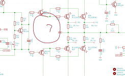
Of the outputs? R26/20/21/9? The 0.1 ohms?
Those are in place on the PCB.
OH r18. Let me check
I was referring to C5 and R18 in your simulation schematic.
HOLY ****.I don't see the resister between the emitters of the driver transistors...do you have it on the assembled board?
I can't believe I missed this. I never put this on the schematic in KiCad...
I think my best course of action is hacking that on the board. I will take inventory on my best course of action.
EDIT: Seems like it should be pretty simple.
EDIT2: Going to go on a run, then I will be back and put the 220 ohm between the two emitters and see how much that changes things. Thanks for all your guys' help.
Attachments
Last edited:
The diff-amp transistors (and any that operates at the 100mW level) should be 300MHz, mpsa56 are much slower. Remember that you have to "cover" all the other poles in the feedback with the dominant pole, so the higher those other poles are then the less compensation and the faster the amp /QUOTE]
According to On Semiconductor datasheet for MPSA56, the fT at 2m.A. ,the mean level of current in each LTP half, is a smidgen over 50MHz
HOLY ****.
I can't believe I missed this. I never put this on the schematic in KiCad...
I think my best course of action is hacking that on the board. I will take inventory on my best course of action.
EDIT: Seems like it should be pretty simple.
EDIT2: Going to go on a run, then I will be back and put the 220 ohm between the two emitters and see how much that changes things. Thanks for all your guys' help.
The palm goes to nattawa for shedding light on the luce.
I called my version of your circuit luceunit odd that it turns out there was a loose unit in there.
100 ohm resistor, R4, next to feedback cap
R4 is just for breaking the ground loop. You don't have loop in a first place. End up you broke the ground. You have to connect DIFFGND to GND at some point, through metal chassis or a wire. For example, join them with wires at the transformer middle point.
HOLY ****.
I can't believe I missed this. I never put this on the schematic in KiCad...
Didn't expect a dramatic turn like this 😀 another proof of "when simulation says it's good, sniff on the layout and assembly"?
Haha, love the naming convention, and thanks for all your help. Just got back from my run going to shower and see how much this 220 ohm changes things.The palm goes to nattawa for shedding light on the luce.
I called my version of your circuit luceunit odd that it turns out there was a loose unit in there.
I'm sorry, R4 is connected to DIFFGND and GND through the ground plane. GND through the ground plane refers back to the power supply. Am I understanding what you are saying correctly?R4 is just for breaking the ground loop. You don't have loop in a first place. End up you broke the ground. You have to connect DIFFGND to GND at some point, through metal chassis or a wire. For example, join them with wires at the transformer middle point.
Very acute observation nattawa, thanks for all your help. Going to shower and make the modification, see how much it changes things. Thanks again.Didn't expect a dramatic turn like this 😀 another proof of "when simulation says it's good, sniff on the layout and assembly"?
Very acute observation nattawa, thanks for all your help. Going to shower and make the modification, see how much it changes things. Thanks again.
No problemo. R18 may not be the answer. I yanked it and the simulation didn't seem to complain...😉 maybe needed to take a transient analysis run to see....
Yeah... Looking at the scope, not much has changed with the 220 in between the two emitters, I have it running idle right here, just monitoring the temps/bias.No problemo. R18 may not be the answer. I yanked it and the simulation didn't seem to complain...😉 maybe needed to take a transient analysis run to see....
Interestingly, I put the 8 ohm load on it and the oscillation did not seem to diminish like it did before. I'm going to try again just to make sure.
EDIT: Actually, yes it does haha. I'm going to try and do the square wave test again.
Here's the square wave.Yeah... Looking at the scope, not much has changed with the 220 in between the two emitters, I have it running idle right here, just monitoring the temps/bias.
Interestingly, I put the 8 ohm load on it and the oscillation did not seem to diminish like it did before. I'm going to try again just to make sure.
EDIT: Actually, yes it does haha. I'm going to try and do the square wave test again.
Attachments

Haha, love the naming convention, and thanks for all your help. Just got back from my run going to shower and see how much this 220 ohm changes things.
I'm sorry, R4 is connected to DIFFGND and GND through the ground plane. GND through the ground plane refers back to the power supply. Am I understanding what you are saying correctly?
Very acute observation nattawa, thanks for all your help. Going to shower and make the modification, see how much it changes things. Thanks again.
Just back from a 6k morning run myself just cooling off. In retirement life can be good.
I'm jealous, finishing off signal processing masters and I'm looking to start my career at 24.5 this next coming summer.Just back from a 6k morning run myself just cooling off. In retirement life can be good.
I'm jealous, finishing off signal processing masters and I'm looking to start my career at 24.5 this next coming summer.
I could say I'm 28 and I'd very much like that to be true. Unfortunately I have to deduct that from 100. My wife says 27 vice versa - we don't take ourselves or life too seriously.
Here's the square wave.
Removing the 220R cross coupling the driver emitters still leaves two forward diode junctions in each half biased by the same Vbe stuck between the CCS and the Vas. In a sense there are two super gain transistors in each half.
I took a look at the layout and didn't see any show stoppers. The CCS for the LTP also has a 1k2 base stopper but since it is cascoded and sees virtually no signal voltage swing, it most likely would not do any harm. However I would change it to 10R or 22R just for the heck of it.
Next perhaps consider degenerating the VAS? In the schematic posted by mjona, all the MPS transistors get replaced with 2N5401 and 2N5551, which in my LTspice I have Bob Cordell's models for in the library. The loop gain plot shows a big peaking between 10-20 MHz if the VAS transistor emitter goes to power rail straight. 22R (roughly 8x) degeneration removes the peaking quite effectively.
In the PCB layout the PNP driver transistor shares power rail with the emitter of VAS transistor, through a long trace. Not to say it causes troubles but I would never feel comfortable doing that. I'd cut the trace going between the two, then run a fly wire from the e-cap at the power entry directly to the driver transistor collector.
Besides, the usual R-C filters on the power rails for the VAS and front end are also missing in the layout. Again not saying that was behind the trouble in question, they are regarded as a basic housekeeping item.
Unsure about the RC filters on the power rails you are describing.I took a look at the layout and didn't see any show stoppers. The CCS for the LTP also has a 1k2 base stopper but since it is cascoded and sees virtually no signal voltage swing, it most likely would not do any harm. However I would change it to 10R or 22R just for the heck of it.
Next perhaps consider degenerating the VAS? In the schematic posted by mjona, all the MPS transistors get replaced with 2N5401 and 2N5551, which in my LTspice I have Bob Cordell's models for in the library. The loop gain plot shows a big peaking between 10-20 MHz if the VAS transistor emitter goes to power rail straight. 22R (roughly 8x) degeneration removes the peaking quite effectively.
In the PCB layout the PNP driver transistor shares power rail with the emitter of VAS transistor, through a long trace. Not to say it causes troubles but I would never feel comfortable doing that. I'd cut the trace going between the two, then run a fly wire from the e-cap at the power entry directly to the driver transistor collector.
Besides, the usual R-C filters on the power rails for the VAS and front end are also missing in the layout. Again not saying that was behind the trouble in question, they are regarded as a basic housekeeping item.
I picked up the 2.2 ohm resistors and am about to swap them out. I'll also degenerate Q14 with 33 ohms. Be back in a sec.
First observation: replaced the base stoppers to their appropriate value of 2.2 ohms. Oscillation at 16 MHz did not stop, actually it's now 90 mVrms, or 300 mVpp, which is larger than it was with the 22 ohm base stoppers in. Another interesting observation is that the original bias adjustment I had for about a 50 mV drop across the emitter resistors was wayyy off in this new configuration. This makes sense, as we have less dissipation in these base stopper resistors, so I had to turn the bias down. Also, the Vbe multiplier (bias) seems to be more aggressive, which kind of makes sense as well... Going to try and degenerate the VAS transistor now and see if that makes a difference.Unsure about the RC filters on the power rails you are describing.
I picked up the 2.2 ohm resistors and am about to swap them out. I'll also degenerate Q14 with 33 ohms. Be back in a sec.
EDIT 1: Degenerating Q14 with 22 ohms did not do the trick. I'm going to take a look at degenerating Q16, I'm wondering if that might make a difference.
Last edited:
I took a look at the layout and didn't see any show stoppers. The CCS for the LTP also has a 1k2 base stopper but since it is cascoded and sees virtually no signal voltage swing, it most likely would not do any harm. However I would change it to 10R or 22R just for the heck of it.
Next perhaps consider degenerating the VAS? In the schematic posted by mjona, all the MPS transistors get replaced with 2N5401 and 2N5551, which in my LTspice I have Bob Cordell's models for in the library. The loop gain plot shows a big peaking between 10-20 MHz if the VAS transistor emitter goes to power rail straight. 22R (roughly 8x) degeneration removes the peaking quite effectively.
The Tian plot looks a lot better with a change in the CCS configuration where the transistors have been changed to 2N2907 good enough for simulation purposes.
I have looked back through some old magazines to find an article "Sources 101: Audio Current Regulator Tests for High Performance" part 1 published by AudioXpress issue of April 2007 - authored by Walt Jung
This PNP type actually 2N2907A is quoted b him as representing a sweet spot of performance for these applications - excellent rejection for low frequencies, yet still low-to-moderate capacitance which allows good performance to hold up well with frequency at great prices. They allow currents from low u.A. levels up to 20 m.A. or more at levels of 40V (or more). The matching NPN is 2222A
2N2907 is an oldie and a goodie that hobby electronics stores should have in stock.
The second change is to move the stopper resistor value changed to 100R so it sits in the base connection of Q10 and Q14.
I have rearranged the Vi and Ii inputs so these are ahead of the zobel network.
Attachments
Hi mjona, if you bias the output stage to a more realistic idle current, say in the neighborhood of 100 mA per transistor, the peaking in the loop gain plot shows up, even with the goodie 2N2907. a 20R degeneration at emitter of VAS makes it go away.
Do you think degenerating the Q16 of the CCS for the VAS could affect the peaking? I degenerated Q14 and the oscillation did not go away.Hi mjona, if you bias the output stage to a more realistic idle current, say in the neighborhood of 100 mA per transistor, the peaking in the loop gain plot shows up, even with the goodie 2N2907. a 20R degeneration at emitter of VAS makes it go away.
EDIT: I'm wondering too if a base stopper between Q16 and emitter of Q14 is necessary.
Last edited:
- Home
- Amplifiers
- Solid State
- Is this too much ringing?