It was my understanding that while earthing the heatsink within a chassis is a necessary safety practice (also necessary while prototyping in a higher voltage environment), troubleshooting the amplifier before mounting everything in a chassis was the correct approach.
Do you think earthing the heatsink will solve my oscillation problem?
EDIT: I've attached a plot for gain and phase margin, a little unsure if that hump of phase is bad / how it affects reading off the phase/gain margin.
Also, am I correct in saying those rolloff points are poles?
16 MHz lies on -9.57 dB of the bode plot, is this my feedback factor? 22k / 1.2k?
There is a good thread dealing with earthing that you can learn from here How to wire up an Amplifier
I suggest you get on with the task of arranging your electronics within a chassis incorporating the lessons in that thread.
Somewhere in a recent post someone found his stability problems disappeared once the heat sink was in electrical contact with the chassis but there are some other aspects to consider too that can be looked at when you have everything assembled as above.
With four output devices per module it looks to me that your project is based on an application for a higher power amplifier running off roughly double the voltage of your supplies.
This led me to suggest increasing the Miller capacitor value from 100 pF to 150 pF.
The collector to base diffusion capacitance has an inverse relationship to the square root of the voltage appearing at the collector - so this capacitance is parasitic and non-linear.
A linear capacitor sufficiently large in value will swamp that out. 100 pF works in a simulation but sometimes things don't work out as they should.
Early Motorola application notes that I still have left the value for builders to work out by trial and error. You might have to do that but flag that as wait and see.
With regard to the base emitter capacitance this is directly proportional to the emitter current so the value of this will increase with high power use which calls for discretion with the values of base stopper resistors.
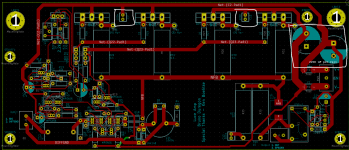
For some reason the image of your board shows you have not gotten around to reducing the value from 22R to 2R2.
I see.There is a good thread dealing with earthing that you can learn from here How to wire up an Amplifier
I suggest you get on with the task of arranging your electronics within a chassis incorporating the lessons in that thread.
Somewhere in a recent post someone found his stability problems disappeared once the heat sink was in electrical contact with the chassis but there are some other aspects to consider too that can be looked at when you have everything assembled as above.
With four output devices per module it looks to me that your project is based on an application for a higher power amplifier running off roughly double the voltage of your supplies.
This led me to suggest increasing the Miller capacitor value from 100 pF to 150 pF.
The collector to base diffusion capacitance has an inverse relationship to the square root of the voltage appearing at the collector - so this capacitance is parasitic and non-linear.
A linear capacitor sufficiently large in value will swamp that out. 100 pF works in a simulation but sometimes things don't work out as they should.
Early Motorola application notes that I still have left the value for builders to work out by trial and error. You might have to do that but flag that as wait and see.
With regard to the base emitter capacitance this is directly proportional to the emitter current so the value of this will increase with high power use which calls for discretion with the values of base stopper resistors.
For some reason the image of your board shows you have not gotten around to reducing the value from 22R to 2R2.
The amplifier was not based on any higher power application, I started with 30 V rails while designing, and decided to add in two output pairs to seemingly handle output capabilities effortlessly, instead of putting all the pressure on one output pair.
I haven't had the chance to get the 2.2 ohm resistors yet, either tomorrow I will be able to or on Friday. I will take a look and play around in the sim some more. I need to spend more time looking at feedback factor, how much gain/phase margin I have, and why I'm oscillating at 16 MHz.
Thanks for all your help.
I see.
The amplifier was not based on any higher power application, I started with 30 V rails while designing, and decided to add in two output pairs to seemingly handle output capabilities effortlessly, instead of putting all the pressure on one output pair.
I haven't had the chance to get the 2.2 ohm resistors yet, either tomorrow I will be able to or on Friday. I will take a look and play around in the sim some more. I need to spend more time looking at feedback factor, how much gain/phase margin I have, and why I'm oscillating at 16 MHz.
Thanks for all your help.
I looked at the circuit using Cordell .models and could not see the issue at 16MHz in your simulation.
This could be down to differences in .models used - some people don't trust those provided on manufacturers websites.
The .asc is attached. After you click run click on vout in the header of the .raw file that results, delete V(vout) in that space and then paste in
-1/(1-1/(2*(I(Vi)@1*V(x)@2-V(x)@1*I(Vi)@2)+V(x)@1+I(Vi)@2)).
I have left that in a comment field on the .asc file where it can be copied.
Also in that dialogue box select cursors 1&2 and click enter.
In the next window drag these cursors to 0dB and -180 degrees. Use the side arrow keys for fine adjustments.
The dialogue can also be dragged for more convenient viewing.
My simulation encompasses the whole circuit including the rf low pass input filter.
The the stability margins look good however the gain at 1Hz is very high so there is a lot of feedback and layout is important.
The gain slope has the shape of a kneecap in a part which looks irregular.
Attachments
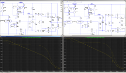
I replaced the CCS in VAS stage with an ideal current source and the loop gain plot is all smooth. Perhaps worth a bit more exploration into the CCS circuit. See the attached screenshot of after-before side-by-side.
p.s. reducing the base stopper at the CCS (R16) from 1k2 to 47R also smooths out the loop gain plot completely.
p.s. reducing the base stopper at the CCS (R16) from 1k2 to 47R also smooths out the loop gain plot completely.
Attachments
Last edited:
In the schematic on the left, did you change R16 to 47?I replaced the CCS in VAS stage with an ideal current source and the loop gain plot is all smooth. Perhaps worth a bit more exploration into the CCS circuit. See the attached screenshot of after-before side-by-side.
p.s. reducing the base stopper at the CCS (R16) from 1k2 to 47R also smooths out the loop gain plot completely.
EDIT: just realized that's the picture with the ideal current source, my bad.
Last edited:
Thank you for the loop gain expression. I noticed in your schematic, you're taking the feedback point from after the zobel network. Is that correct? It was explained to me you put the zobel AFTER the feedback.I looked at the circuit using Cordell .models and could not see the issue at 16MHz in your simulation.
This could be down to differences in .models used - some people don't trust those provided on manufacturers websites.
The .asc is attached. After you click run click on vout in the header of the .raw file that results, delete V(vout) in that space and then paste in
-1/(1-1/(2*(I(Vi)@1*V(x)@2-V(x)@1*I(Vi)@2)+V(x)@1+I(Vi)@2)).
I have left that in a comment field on the .asc file where it can be copied.
Also in that dialogue box select cursors 1&2 and click enter.
In the next window drag these cursors to 0dB and -180 degrees. Use the side arrow keys for fine adjustments.
The dialogue can also be dragged for more convenient viewing.
My simulation encompasses the whole circuit including the rf low pass input filter.
The the stability margins look good however the gain at 1Hz is very high so there is a lot of feedback and layout is important.
The gain slope has the shape of a kneecap in a part which looks irregular.
In the schematic on the left, did you change R16 to 47?
No, I didn't. In that screenshot the left side has the CCS disconnected and the VAS is instead loaded with an ideal current source I2 (7.1 mA).
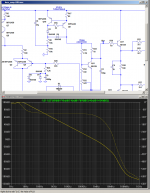
Please see attached screenshot with R16 changed to 22R. Since the loop gain plot starts to have this "wrinkle" at R16 = 68R, I would not use anything higher than 22R.
Attachments
I edited my post after realizing my mistake, my bad. I'm trying to play around with this in my sim, but cannot seem to get the same responses that you and mojona are looking at. I altered his schematic to take the feedback path from before the zobel, and looking at loopgain2.asc from the LTSpice examples, I'm trying to get the correct positioning of the probes.No, I didn't. In that screenshot the left side has the CCS disconnected and the VAS is instead loaded with an ideal current source I2 (7.1 mA).
Please see attached screenshot with R16 changed to 22R. Since the loop gain plot starts to have this "wrinkle" at R16 = 68R, I would not use anything higher than 22R.
Attachments
I edited my post after realizing my mistake, my bad. I'm trying to play around with this in my sim, but cannot seem to get the same responses that you and mojona are looking at. I altered his schematic to take the feedback path from before the zobel, and looking at loopgain2.asc from the LTSpice examples, I'm trying to get the correct positioning of the probes.
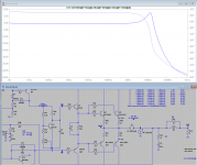
I put in the probe like this:
Attachments

Ah! I found my mistake, my input voltage source was AC 1, instead of 0.I put in the probe like this:
In sims, it seems I have a 75 degree phase margin, seems okay. Just taking a look at the frequency response after the zobel network, I don't see the 16 MHz oscillation either anymore.
On the bench, I changed the 1.2k base stopper to 22 and I'm still seeing the 16 MHz oscillation. But, I still haven't changed all the 22 base stoppers in the driver and output to 2.2, so there's that. Going to keep investigating.
EDIT: here's a probably not trustworthy FFT
EDIT2: Also, even with the 22 ohm base stoppers in, and everything like how I have it in real life, I don't see the 16 MHz peaking in the direct frequency response from the output (in sim) anymore.
EDIT3: I just put my dummy 8 ohm load on the output. The oscillation goes from 177 mVpp to like 16 mVpp. I'm going to try the square wave test again and see if it looks any better.
Attachments

Last edited:
An input filter is not part of the feedback system, and doesn't affect stability.
The ~decoupling impedance of the input transistor base is part of the feedback loop. The 33pF cap moves the input transistor pole up and away from the dominant pole. The diff-amp transistors (and any that operates at the 100mW level) should be 300MHz, mpsa56 are much slower. Remember that you have to "cover" all the other poles in the feedback with the dominant pole, so the higher those other poles are then the less compensation and the faster the amp.
A similar problem happens at the negative input when the feedback network uses high resistance values. A pair of RC networks can reduce the feedback impedance and maintain the feedback ratio. Some just use low value feedback resistors but that requires a high wattage resistor on the top side if the divider.
Be careful that "base blocker"resistors are not creating unnecessary phase lag that destabilizes the feedback.
Okay thanks.The ~decoupling impedance of the input transistor base is part of the feedback loop. The 33pF cap moves the input transistor pole up and away from the dominant pole. The diff-amp transistors (and any that operates at the 100mW level) should be 300MHz, mpsa56 are much slower. Remember that you have to "cover" all the other poles in the feedback with the dominant pole, so the higher those other poles are then the less compensation and the faster the amp.
A similar problem happens at the negative input when the feedback network uses high resistance values. A pair of RC networks can reduce the feedback impedance and maintain the feedback ratio. Some just use low value feedback resistors but that requires a high wattage resistor on the top side if the divider.
Be careful that "base blocker"resistors are not creating unnecessary phase lag that destabilizes the feedback.
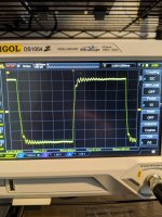
This is the square wave response after the third edit in post 50.
8 Ohm load, 100 mVpp 10 kHz square wave. Input filter of 10k and 0.1 uF before the 2.2 uF coupling cap.
Attachments
You do have decoupling capacitors in place on your PCB (C3 and C4), right?
From nattawa's plot, it should be pretty stable. Sometime, absence of decoupling will make weird things.
From nattawa's plot, it should be pretty stable. Sometime, absence of decoupling will make weird things.
Yes.You do have decoupling capacitors in place on your PCB (C3 and C4), right?
From nattawa's plot, it should be pretty stable. Sometime, absence of decoupling will make weird things.
Attachments
About the current source: Q9+Q16 can be unstable unless you include a base resistor for Q16 or a cap across the C-E. Same thing applies to the LTP/ diff-amp current source.
I see what you were saying earlier about the MPSA56/06 being kind of slow. I'll do more research next time I'm picking those out.About the current source: Q9+Q16 can be unstable unless you include a base resistor for Q16 or a cap across the C-E. Same thing applies to the LTP/ diff-amp current source.
I could rip up a trace or do some funky stuff to get a resistor in between Q9 and Q16. I've tried putting a cap across CE of Q19 before, and it didn't change the 16 MHz oscillation at all. Tried 0.1 uF ceramic and 47 uF electrolytic. I could try again though.
Do you connect DIFFGND of input and GND of Power together at some where?
I remember from one of your photo, DIFFGND just is floating there. The amp will not work correctly if you leave DIFFGND floating.
I remember from one of your photo, DIFFGND just is floating there. The amp will not work correctly if you leave DIFFGND floating.
100 ohm resistor, R4, next to feedback capDo you connect DIFFGND of input and GND of Power together at some where?
I remember from one of your photo, DIFFGND just is floating there. The amp will not work correctly if you leave DIFFGND floating.
I don't see the resister between the emitters of the driver transistors...do you have it on the assembled board?
Of the outputs? R26/20/21/9? The 0.1 ohms?I don't see the resister between the emitters of the driver transistors...do you have it on the assembled board?
Those are in place on the PCB.
OH r18. Let me check
- Home
- Amplifiers
- Solid State
- Is this too much ringing?