It is a pity that today, losing those who are interested in how that works.
Federmann,
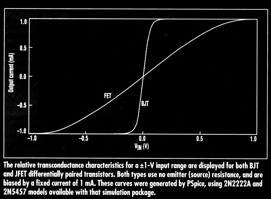
take a look at the picture above... so if we understand you correct, you would like to have "gain reserve" with BJT as like the FET curve which is wide?
Then if you put emitter resistors to the BJT in the differential stage you will get the curve looking like the curve for FET as the picture shows.
If you simulate you will see!
Cheers Michael
OK guys, it was my pleasure to spend my time here with you in this fruitful discussion. I will apologize now and put it completely into trustful Federmann's hands.
I am not claiming that the phase shift caused by bias. I say that:
1st Phase shift indicates a ratio amplifier and a decrease in amplification.
2nd The decrease in gain less suppress non-linearity amplifier.
3rd The decrease in gain increases Vdif.
4th Vdif gets into the nonlinear region.
5th Cause the nonlinear, then modulation.
The worst situation occurs when large changes in audio signals and high harmonics.
I say that the phase shift may be a measure of quality amplifiers. We need to know the involvement of input circuits and the size of the output voltage.
Federmann,
take a look at the picture above... so if we understand you correct, you would like to have "gain reserve" with BJT as like the FET curve which is wide?
Then if you put emitter resistors to the BJT in the differential stage you will get the curve looking like the curve for FET as the picture shows.
If you simulate you will see!
Cheers Michael
Michael This is not the best solution, resistors reduce amplification and the result is greater Vdif.
Michael This is not the best solution, resistors reduce amplification and the result is greater Vdif.
Is true the amplification (gain) goes down, but you forget to mention one thing, the linearity goes up!
So what do you prefer, high gain or high linearity?
Cheers Michael
So what do you prefer, high gain or high linearity?
Appropriate combination of gain and linearity
That is correct Federmann, we don't need to put very "large value" resistor on the emitter as we will lose gain, but we still want to have some linearity, this means we have to at least use a "small value" resistor on the emitter so we can have both appropriate combination of gain and linearity. 
The same with VAS (Voltage Amplification Stage), it needs also an appropriate emitter resistor.
And the same with output transistor.
It will make them all more linear and also much better temperature stability.
Cheers Michael
The same with VAS (Voltage Amplification Stage), it needs also an appropriate emitter resistor.
And the same with output transistor.
It will make them all more linear and also much better temperature stability.
Cheers Michael
Better course Vdif and greater amplification can be achieved more current. Increasing enlarge the symmetrical involvement.
Another thing I would like to point out in the HQQF design, in the current schematic there is only one gate resistor shared by all four MOSFET output transistor.
100 Ohm in this point is the same as if 400 Ohm is connected to each MOSFETs gate, this is a very high value.
We have to remember the Miller capacitance inside the MOSFET are quite large and very non-linear, to mitigate the non-linear effect and at the same time increase speed of output transistors the gate resistor value has to be decreased.
You can put 100 Ohm gate resistor to each MOSFETs gate, this will equal to 25 Ohm in the current position you have in your schematic.
Now you will have a rocket amplifier!
Cheers Michael
Last edited:
I know very well, it is worth to be determined by the selection transistors. Similarly, the size of emitorových resistance. Unless transistors within ± 1%, the emitter resistors. Similarly, zener diodes are selected. There are many things that were not written. There are many things that depend on the choice of transistors.
The amplifier has played very well. Amplifier waiting for precise measurements and settings. Then publish the details.
The situation is still unresolved, Bob, even if you slowed things down a bit.
Hi John,
It is certainly unresolved in you mind. Just by saying it is so, does not make it so, John. You don't back up your assertions with technical arguments.
I think that where you miss the boat is that you don't compare apples to apples when talking of high and low open loop bandwidth. It is certainly true that if you double the size of the compensation capacitor, open loop bandwidth will be reduced and PIM will be increased. However, if you stop there, you are not comparing apples to apples. A proper apples-to-apples comparison keeps the closed loop bandwidth of the design the same. Once you keep the closed loop bandwidths the same, you see that open loop bandwidth goes out of the equation. Bear in mind that the gain-bandwidth of the aplifier is what counts, and that variation of LTP gain with signal varies the gain-bandwidth product, which in turn varies the closed loop bandwidth, corresponding to a pole at the gain crossover frequency that moves about with program material. The phase change that this pole movement causes in-band is what causes PIM.
You seem not to understand that open loop bandwidth does not necessarily have any bearing on gain-bandwidth product or closed loop pole position.
Perhaps the key to your lack of understanding is your failure to recognize that amplifiers with low open loop bandwidth are that way because they naturally have higher low-frequency gain, thus keeping the gain crossover frequency the same as a wide open-loop bandwidth amplifier with less DC gain. If you focus instead on the amount of loop gain at 20 kHz being the same you will come closer to understanding what does and does not affect PIM.
Do you not agree that movement of the closed loop pole is what causes PIM in a feedback amplifier?
Cheers,
Bob
Do you not agree that movement of the closed loop pole is what causes PIM in a feedback amplifier?
Cheers,
Bob
That is the point, of course.
Regards,
I'm thinking maybe you misunderstood the latter part of my post.
I am interested whether or not the NTP (blue trace) performs better or worse than the LTP in terms of this odd modulation distortion. I am thankful for the help plotting derivatives and such, since even though it is not what I had in mind I've learned some things that will come in handy.
I would like those who haven't/won't contribute anything meaningful to leave. If I want to do my own research on the subject, I want to do it in peace without several arbitrary voices decreasing the S/N ratio. (if Federman is wrong, I will find out myself!)
I'm working on plotting some more solid data...
- keantoken
Do you have any new findings please?
This thread is quite an embarasment. I salute those who want to keep it on track.
Thank you for greeting and wish you a nice Christmas and new year.
I salute those who want to keep it on track.
Can I ask how you like comments Vdif ≈ U1 * sin α
• U1 = Input voltage amplifier.
• α = phase shift of output voltage amplifier.
• Evaluation amplifier without the input and output filter.
Somebody isn't convincible even by greatest experts....🙂
This is not about persuasion, it is about basic knowledge of mathematics.
- Status
- Not open for further replies.
- Home
- Amplifiers
- Solid State
- Influence of the delay amplifiers for listening characteristics