The scheme in #18 is not workable, as there is no bias feedback to the opamp. Having a transformer imbedded within a global feedback design will considerably complicate the design and the effort required.
Unless you're determined to design your own amp for the learning experience, I'd advise building a proven design.
Unless you're determined to design your own amp for the learning experience, I'd advise building a proven design.

My (somewhat limited) experience is that involving an opamp creates more problems than it solves. One solution is to bootstrap the opamp, i.e. let the supply voltage follow the output. This is discussed in this article: https://www.analog.com/en/resources/analog-dialogue/raqs/raq-issue-168.html
I would personally ditch the opamp and go with a classic LTP differential stage. There’s a lot of MOSFET based designs out there that you can adapt to laterals and some that already features them.
I would personally ditch the opamp and go with a classic LTP differential stage. There’s a lot of MOSFET based designs out there that you can adapt to laterals and some that already features them.
For giggles I added the SPICE models for some Exicon laterals to my Bog Standard project. I had to adjust the VBE quite a bit to get the right bias but it works. The THD went up slightly, but there's probably more adjustments needed. Again, totally for giggles, but here's the SPICE file: https://github.com/prydin/the-bog-standard/tree/main/spice
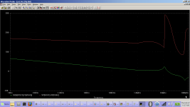
This kind of transformers.


I like using opamps to lower noise and THD like composite LM3886.
Until yet no schematic found with specs as in post 1.
I like using opamps to lower noise and THD like composite LM3886.
Until yet no schematic found with specs as in post 1.
I’m not necessarily 100% on board with the statement that opamps always give you lower noise and THD…
I did not said always, but all the amps with extreme low noise and thd using massive high bandwidth feedback.
I have 16W amp see below with opa1611 as correction opamp.
THD+Noise below 0.00008% at 1W 8ohm.

I have 16W amp see below with opa1611 as correction opamp.
THD+Noise below 0.00008% at 1W 8ohm.
Last edited:
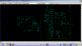
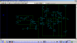
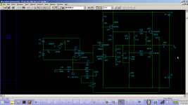
How is the bias set? I like to start with 400mA and +/-36v power supply.Something like this has possibilities. It has a gain of 2 and it swings to the rails. Some or all of the components need some adjustment.
The bias is set by the collector current of Q27 going through R33 which creates gate voltage for Fet16 and Fet17. I have no models or simulations to actually have real values. I don't know how stable the bias point will be because of Q27 heating effects. Ideally Q26 and Q27 need to be at the same temperature so that the voltage across R33 would be nearly temperature independent. The voltage across R33 is VR33=R33*{R31*(Vrail-Vbe26)/(R34+R22+R31)+Vbe26-Vbe27}/R32.
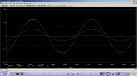
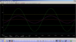
You made me go to work. Here is some data. I think that I have the right models but someone will have to check me. The bias is at 400ma. I am using a 13v/us op_amp model. It needs about a gain of 3 in the output stage to work well. I had to compensate the output stage for stability. It may have issues but it does amplify with low distortion. I used some transistor models from a collection by Bob Cordell for the simulation.
Attachments
Many thanks for the effort, I needed this kind of effort/support.
The gate/source op the 10n20 needs capacity compensation by adding a capacitors of 390p. The 10p20 has already this higher Cgs. Maybe distortion will be better.
I will study your proposal and make a PCB to build and test.
The gate/source op the 10n20 needs capacity compensation by adding a capacitors of 390p. The 10p20 has already this higher Cgs. Maybe distortion will be better.
I will study your proposal and make a PCB to build and test.
The opamp you use for high bandwidth error correction by feedback to get lower thd and noise, psrr then without opamp.
It is possible to get almost same thd + n specs as the opamp.
Just look at composite lm3886 designs with specs better then standalone lm3886.
I expect with this topology get at least ten times better figures then normal lat fet designs.
It is possible to get almost same thd + n specs as the opamp.
Just look at composite lm3886 designs with specs better then standalone lm3886.
I expect with this topology get at least ten times better figures then normal lat fet designs.
I think it will self oscillate.
You have three amplifier stages. First the Op with a 0 db gain at 7,2MHz. Then comes the transistor stage with a bandwith of about 0,7 MHz and then the LATfet stage with a varying bandwith depending of the D-S voltage but something like 1,5 to 3 MHz. I have not made a simulation but to me it looks like a lot of phase shift. If you google "nested Miller integrators" You will find a method of getting following integrating stages to work.
You have three amplifier stages. First the Op with a 0 db gain at 7,2MHz. Then comes the transistor stage with a bandwith of about 0,7 MHz and then the LATfet stage with a varying bandwith depending of the D-S voltage but something like 1,5 to 3 MHz. I have not made a simulation but to me it looks like a lot of phase shift. If you google "nested Miller integrators" You will find a method of getting following integrating stages to work.
You are right when this is not right suppressed. That is why simulating can help to find just the right phase margin.
Thanks.
Normaly I would remove C1 and optimize C6.
What is the Ibias in your simulation? Is Vgs about 1V?
Normaly I would remove C1 and optimize C6.
What is the Ibias in your simulation? Is Vgs about 1V?
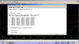
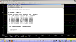
The upper N channel fet has 0.973 Vgs and the lower P channel fet has 1.128v Vgs with a 0.394A bias.
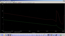
You can't be sure of the AC analysis because I don't have the real model of your op-amp. So be aware that you may want or need to change some values when you have the actual circuit.
You can't be sure of the AC analysis because I don't have the real model of your op-amp. So be aware that you may want or need to change some values when you have the actual circuit.
Last edited:
- Home
- Amplifiers
- Solid State
- Help, with LAT FET schematic