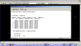
I ran a simulation at 5 Watt Rms with 8 ohms and measured a TOTAL HARMONIC DISTORTION = 4.804586E-04 PERCENT. You might get better with your op_amp but you can't do too much better because of the band width limit of the output stage. 5 parts out of a million isn't too bad.
Attachments
I made this a few years ago.
I dissmissed it because it was not good enough in higher frequencies. Distortion was about 1 or 2 ppm at 1kHz with OPA1655.
OPA1655 is not good for power amplifiers because its output stage has internal high impedance and a non linear load makes it distort.
Maybe it will work better with latfet.

I dissmissed it because it was not good enough in higher frequencies. Distortion was about 1 or 2 ppm at 1kHz with OPA1655.
OPA1655 is not good for power amplifiers because its output stage has internal high impedance and a non linear load makes it distort.
Maybe it will work better with latfet.
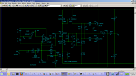
Stigigemla, in your schematic with input on inverting input of the opamp you got very low input impedance of 390 ohm.
Latest version


Latest version
Last edited:
The amplifier is noninverting having 91,23 k ohm in.
I am using TINA from Texas.
I do not get adequat distortion levels in it but believes thats from bad spice models.
I am using TINA from Texas.
I do not get adequat distortion levels in it but believes thats from bad spice models.
Designspark PCB,it is for free.What PCB software do you use?
Made my own symbol library.

Your drawing shows input on “-“, then R5//R3 is your input impedance.The amplifier is noninverting having 91,23 k ohm in.
I am using TINA from Texas.
I do not get adequat distortion levels in it but believes thats from bad spice models.
Last edited:
It is more serios than that. I wanted to see T1 and T2 with input on the base
and forgot the phase reversal when i cleaned the schematic after that.
Here is the correct schematic.

and forgot the phase reversal when i cleaned the schematic after that.
Here is the correct schematic.
No. With the low voltage the Op stay cooler and that is positive for input voltage noise. The low voltage ensures also that the bipolar transistors dont burn at over drive or current limit in the output stage. (not included in this schematic.)The Op delivers voltage enough for max output at any frequency with the original OP (OPA 1655) The OPA 827 has a little smaller max output voltage so with that maybe 6,8v can be better. ( At 0,5 to 2MHz). R13 + 14 must then increase to keep the current in T3 + 5 at about 10 mA. And the open loop gain will be a little bit smaller.
Last edited:
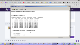
Here is some data on the distortion. I may not understand how to interpret the distortion because it looks like it is better than 2 parts per million but the software says that it is 8 parts per million. The second and largest harmonic is much bigger than the second harmonic in the error ripple.
Attachments
I learned to do my own simulation. Looks realy nice.
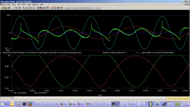
1 Watt output at 8 ohm.

1 Watt output at 8 ohm.
Prove of concept.
Today I finally time to finish the board and test it.

First measurements are:

Later this week I will do THD measurements, maybe first build it in a nice case.
Below the gerbers I used.
Today I finally time to finish the board and test it.
First measurements are:
- DC at output = 0,3 mv.
- Clipping starts at 21Vrms in 8 Ohm.(1khz)
- Ibias is adjustable from 0...1,5A(set on 500mA).
- Voltage used +/- 36V.
Later this week I will do THD measurements, maybe first build it in a nice case.
Below the gerbers I used.
Attachments
Realy good distorsion figures(0.000058%) at 1W 8ohm. Just need to lower 50Hz interference with measurement.

That bias spreader is a recipe for trouble. If the wiper of the trimpot lets go, the bias goes high, which causes the output stage to blow. I suggest this modification:I made this a few years ago.
This way if the wiper disconnects – which is the most common failure mode for a trimpot – T4 conduct more and reduce the bias of the output stage.
Tom
- Home
- Amplifiers
- Solid State
- Help, with LAT FET schematic