Nice work!
Some thoughts.
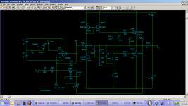
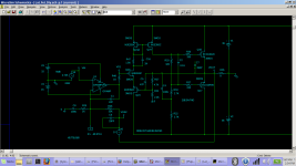
Some Miller capacitance at Q24 gate to drain might tame the gain peak in the output stage. The capacitor at the output MOSFET gate may aggravate the phase shift. You might try removing in simulation.
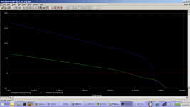
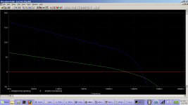
The output section has voltage gain of about 3 and adds phase shift. Both act to reduce gain/phase margins. C6 aggravates this issue but C1 helps stabilize.
Some thoughts.
Some Miller capacitance at Q24 gate to drain might tame the gain peak in the output stage. The capacitor at the output MOSFET gate may aggravate the phase shift. You might try removing in simulation.
The output section has voltage gain of about 3 and adds phase shift. Both act to reduce gain/phase margins. C6 aggravates this issue but C1 helps stabilize.

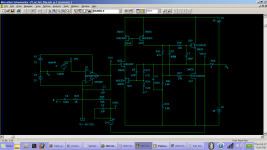
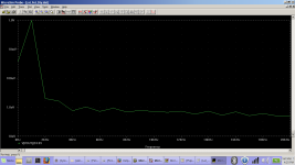
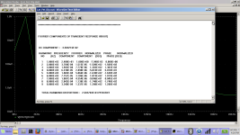
I discovered a better point to tie the compensation capacitor of the 3x gain amplifier. Also, I tried a version with a current mirror to see if it was more stable. The current mirror version appears to be more stable but it requires a transistor instead of a resistor. If another transistor is acceptable then you can consider version A. It yields TOTAL HARMONIC DISTORTION = 5.129679E-04 PERCENT. I second guess myself and I am not sure which version is better. Maybe you could make a layout that can use either a resistor or a transistor just in case one version proves to be better.
Attachments


Last edited:
Capacitor on Q1(Q16) compensates Cgs between 10n20 and 10p20. Now both have same Cgs.
I make PCB as universal as possible and go for most stable version but still can ad other options.
I make PCB as universal as possible and go for most stable version but still can ad other options.
That changes the gain response for the N channel mosfet at around 30Mhz, which will also effect the loop gain and phase response of the amplifier.Capacitor on Q1(Q16) compensates Cgs between 10n20 and 10p20. Now both have same Cgs.
The proper way to compensate is to have different gate resistor values, typically 470R for the N channel and 220R for the P channel.
You will need to re-run your circuit simulator to check the loop gain and phase margins and adjust as necessary.
What I meant by "adjust as necessary", I was referring to changing the compensation capacitors C3,C4 and C25 to adjust the loop gain and phase after changing the resistors R9 to 470R and R10 to 220R.
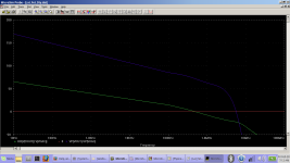
C23 doesn't actually roll the gain off for the N channel mosfet, it puts a null in the gain response at around 30Mhz. With C23 having a value of 390pf and depending on the bias the N channel will have a 20db null in gain compared to the P channel at around 30Mhz.
With the change to the value of the gate resistors, the gain for both mosfets will roll off at the same rate.

I'm still working with the design. I would like another day or so to see if I can remove the gain of 3 amplifier. If you are really in a hurry then you can build it but I may have another solution that is more stable.
Good idea James361, just take the time. Making PCB’s cost( 4 euro for 5 pieces shipment included) almost nothing. Often it takes several iterations. I like to have already a platform(pcb) to test ideas.
I have a few suggestions about the PCB design.
First i would move the power rail inductor to the PSU board to minmise the influence of the magnetic fields in the amplifier.
Then i would move the power inputs to the other side of the big electrolytics to minimise the magnetic fields again.
The class B part of the current in the output transistors has about 35% distortion so that leads shall also be short and that is very good in your PCB.
The output terminal should I move to the op side of the big electrolytics and make a separate ground lead from it to a ground junction near the input.
From the output terminal i would take a separate lead for the voltage feedback and have OP pin2 and 3 near the ground junction to minimize the possible induction from the output halves and mobile phones etc.
Using the ground plane as a conductor near the input can easily give 0,00x % distortion and sometimes more distortion so all signal ground separate to the junction point.
It is a very interesting topic with the 3 transistor mid stage so i will be happy to see its real potential.
Thanks stigigemia for your remarks.
On the PSU is no place for the inductors, I use a ready made smps.
The current power layout I already used for a previous Trex version(12 watt).
Until yet I have no problems with rf or magnetic fields in all of my builds.
But when it happends, I will think about your remarks.
On the PSU is no place for the inductors, I use a ready made smps.
The current power layout I already used for a previous Trex version(12 watt).
Until yet I have no problems with rf or magnetic fields in all of my builds.
But when it happends, I will think about your remarks.
The magnetic fields can be a reason why distortion in an amp is bigger than simulated.
I have had it in size of about -120dB. I want to see your amp do better than that.
I have had it in size of about -120dB. I want to see your amp do better than that.
That is also the design goal, -120db. For a latfet design 10 times better as I have seen until yet.
I am very curious what will be the result, maybe after some fine tuning.
I am very curious what will be the result, maybe after some fine tuning.
I had an idea about another drive scheme but I could not make it work well. It turns out that the 3x gain circuit gives the lowest distortion results at about 0.003%. I did add 3 more components to the design to protect the 3x amplifier. It can draw high current when the output goes into clipping so I thought that it was important to add 2 resistors for a current limit for the 3x amp. I added a capacitor to bypass one of those resistors to keep the loop stable. I hope that you don't mind the new parts. Also, I lowered the resistors by about half in the output bias stage because I thought that it was slew rate limiting at too low of a frequency. I feel pretty confident in the design now.
Attachments

- Home
- Amplifiers
- Solid State
- Help, with LAT FET schematic