I agree with Charles, a notch can be added without adding an inductor, simply by putting a cap (and perhaps a resistor) in parallel with the main coil. (is that what you meant?) That has a disadvantage, however: the response of the filter remains flat at frequencies higher than the notch freq, so the RFI radiation can become very important.
I thought another way of doing the same, as I have told: adding a second LC stage, calculating the components so the pole is mainly independent on the main filter pole. Then add the notch to this second coil. Then take feedback from the first LC section only (the other has little influence on the overall freq. response and it remains independent on load, so no problem).
BUT: it does not improve the carrier rejection in the feedback loop, only the overall rejection.
SO: I have thought another way: adding the notch in parallel with the FIRST coil, and leaving the second LC stage simple. This way:
a) You have feedback around first filter with improved carrier suppression due to the notch.
b) The filter response continues dropping at high frequencies
c) I get excellent carrier suppression at the output
d) The simulations show about the same phase margin as with single filter and no notch (but THD due to TIM should improve).
e) If the sw. freq. moves away from the notch, you are not worse than you were before (indeed you have to move more than 10% to lose compared with before, so no problem)
What do you think? I am anxious to test that in real-life.
I agree with Charles, a notch can be added without adding an inductor, simply by putting a cap (and perhaps a resistor) in parallel with the main coil.
That's NOT what I meant, since its disadvantages are by far too high.
What I meant was using a notch filter in the signal path before the comparator in order to remove the ripple before the two signals are compared. There are techniques available using simulated inductors or summed high- and lowpass- filters and the like.
Another thing I also once thought of was the use of a tap on the filter coil and a parallel C like below. I want to avoid as many inductors as possible since they are a PITA.
Regards
Charles
Attachments
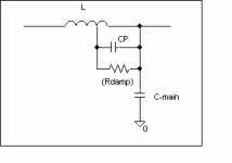
Ah, ok. You meant in the fb. path. (I try to avoid that, due to the phase changes, compensation needs, etc).
Apart from the pain of having another inductor (can be very low valued, a ready-made choke indeed), what do you think of my solution?
Best regards,
Pierre
Apart from the pain of having another inductor (can be very low valued, a ready-made choke indeed), what do you think of my solution?
Best regards,
Pierre
As far as I understood you want to use a notch filter first and then a lowpass, am I right ?
If yes, you might have quite some idle current in your first inductor !
Regards
Charles
If yes, you might have quite some idle current in your first inductor !
Regards
Charles
Yes, that's the idea: the first filter determines the main filter pole, at, say, 50KHz, with a notch at 280KHz or so. The second one is mainly a second pole at, say, 150-200KHz.
Why the high idle current in the first inductor?
Pierre
Why the high idle current in the first inductor?
Pierre
At resonance you always have higher current flowing between inductor and cap than flowing through the parallel arrangement as a whole (also your cap needs to have low losses or it will get hot) !
Now that you connect this thingie directly to the output ..........
Have you simulated it and checked the current ?
Regards
Charles
Now that you connect this thingie directly to the output ..........
Have you simulated it and checked the current ?
Regards
Charles
Ok, I have simulated it quickly, seems to appear huge current peaks in the capacitor, that don't appear if the notch is in the second stage. So I think that Charles is right (as expected), I don't like that currents flowing in my components.
So idea discarded.
To see if we are in the right way (excessive ripple in the feedback signal that causes TIM in the error opamp), perhaps changing it to a very fast one should improve situation, just to be sure that we are not hunting in the wrong direction... what do you think?
I will keep you posted when I can measure something in the prototype.
Pierre
Hi,
I'd like to get an average model going of a full bridge with differential feedback, so that I may properly analyse and tune the feedback loop. Not sure what a good way of doing it is.
Would modelling it as a half bridge with twice the voltage be a viable simplification or is that just a bad idea. Anything else you can tell me to help get me started? Should I start a new thread?
classd4sure
If it´s a triwave amp it should work with a halfbridge with twice the voltage. The ripple becomes the same, the gain as well so it should work.
I don´t understand your problems with the simulation though.
If it´s a triwave amp it should work with a halfbridge with twice the voltage. The ripple becomes the same, the gain as well so it should work.
I don´t understand your problems with the simulation though.
I agree with Pabo on the gain thing. I think the tricky part of the question was how he could take differential feedback from a full-bridge.
There are two ways:
1.) The cheap one:
Take feedback with a differential amplifier e.g. an op-amp. This takes the least amount of components but you have an active component in the feedback path which is suboptimal.
2.) The expensive one:
Build the forward path in a double symmetric way in order to have a symmetric amp from input to output. You then won't have to use active parts in the feedback path you only have them in the forward path.
Regards
Charles
Isn't that "expensive way" that Charles propose very similar to have two half-bridge amplifiers connected in bridge mode?
Best regards
Best regards
Hi,
Pierre, that's exactly right, and that's what it is, but with a single comparator that has quad outputs. It's differentially fed, with the input and output signals summed at both inverting and non inverting comparator inputs.
Both feedback loops are identical.
I'm sure you won't be shocked to hear it's a UCD.
The difference from before is I've fixed the outputs of the comparator this time around and, no op amps at all. I might go for a class A input stage later or I might throw some op amps in for simplicity, but it will only be for the input stage as it will keep fully passive feedback paths this time.
In this case its' probably the inexpensive way because it's only a few more passive components.
I just don't know how to begin modelling that for average mode simulation. Do I use switches for mosfets, or an etable, can I keep the discrete comparator (probably not huh), never done this sort of thing. Can I just use an ideal op amp with alot of gain as the comparator and some ideal switches?
I'll take any links you know of on the topic or anything would be appreciated. I'd like to do this so I can set the gains properly and everything.
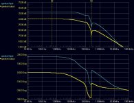
I have changed some components: added 10k resistor in series with the zero in the feedback path, increased integrator's parallel resistor to 180k and capacitor's series resistor to 10k.
This is the output (larger trace) vs input (smaller trace), without averaging, lowpassing, etc.
Output scale is 10V/div on 5 ohms.
This is the output (larger trace) vs input (smaller trace), without averaging, lowpassing, etc.
Output scale is 10V/div on 5 ohms.
Attachments
These are the gate to source voltages of both mosfets.
They have been carefully measured with a 40MHz probe just at the mosfets pins. The scale is 500ns/div, 5V/div.
Top trace is Low side, bottom trace is High side mosfet.
NOTE that the measurements weren't taken at the same time, so they are NOT time aligned!
What do you think?
My gate drive setup is a IR2113 with 10ohm and schottky diodes in antiparallel in series with each gate.
Attachments

As I said, I have changed some values.
I have been doing some careful measurements of the Vds of both mosfets, getting very clean results (but only with 5 ohm load and no signal).
The output is very good visually, but slightly worse at lower frequencies.
The gate waveform seemed a bit slow so I have reduced gate resistors to 6 ohms instead of 10. This seems to have improved low frequency distortion noticeably.
Now the idle current consumption from Vcc (the negative rail has other things that consume power so it is not easy to measure this) is 18mA. I assume that is due to shoot-through. Should that be absolutely zero so I am sure there is no overlap in the mosfets? of it is safe to have some of it so distortion is minimized (like class AB stages)?
Next week I will prepare a setup at home to measure THD with RMAA. I have played with that program a bit in loopback mode and have found that it is very sensitive with the level. It must be very well adjusted for both playback and record (with the volume control panel in Windows) so it can get good results.
Best regards
Pierre
You're using one of the IR driver IC's right?
Ouput current of the driver would be increased from lowering that resistor, not much though, and you still have set dead time so it won't cause overlapping signals.
I can't see how shoot through would increase driver current either.
Due to the driver in use I dont' think you're suffering shoot through caused by overlapping signals, but since you're turning the mosfets on faster with the lower resistor, you give less time for the body diode of the mosfet to recover and that will cause a shoot through like spike, as the mosfet turns on into a partially recovered diode it can't yet fully block the reverse current which gets slammed down it's throat. Big loss of efficiency, would lead to failure. You need the slower turn on to help avoid that.
My simulations have shown massive THD decreases by hugely overlapping the signals... in reality it can never work like that without exploding so a compromise has to be found.
Jaka Racman will be posting some gate driver waveforms for us soon that should be very educational and you may find that helpful in some way. IR gate driver with and without BJT buffers. Stay tunned.
What kind of mosfets are you using anyway?
I have now reduced the gate resistors to 6 ohms and I will post the gate drive signals. They don't show any violent spikes or similar, so I assume they are safe. I think distortion has been greatly reduced, specially noticeable at low frequencies. (all this by eye, still waiting to be able to do some RMAA measurements).
My mosfets are NTP35N15 from OnSemi.
BTW: What signal shoul I watch to in order to ensure that the mosfets are safe? Vgs? Vds?
Best regards,
Pierre
My mosfets are NTP35N15 from OnSemi.
BTW: What signal shoul I watch to in order to ensure that the mosfets are safe? Vgs? Vds?
Best regards,
Pierre
- Status
- Not open for further replies.
- Home
- Amplifiers
- Class D
- Help with feedback