Hi,
You already know your dead time is half decent (drive signals aren't overlapping) due to the nature of your circuit and the driver IC itself, or am I wrong here? If that's the case there's no further need to monitor the gate voltage as far as I know.
Temperature is an indicator, if they run cooler due to the faster transitions, then a lower Ron was well needed. At some point even though the transition is faster it will start to get hotter due to the body diode thing, then you know you've reached a limite with it.
Would be good to monitor Vds but it might be more telling shoot through wise if you can monitor the drop of a few small value resistors in series with either mosfet output.
Jaka Racman just posted those pics, I had no idea those drivers are so weak. Leads one to believe you can remove the resistor altogether, however there's still a need to decouple the gate from circuit inductance. Maybe you should look at adding a buffer to optimize it further?
Regards
Chris
Could you please point to the photos Jaka Racman posted about gate driving? I am curious to see what he got.
Thanks
Thanks
First of all: Congrats to Pierre's and Pete's success regarding perfomance improvements ! 
There is another thing one has to watch out for when dimensioning these gate resistors: Driver dissipation.
When you completely remove the series resistors you do no longer share the losses between driver IC and these resistors. So you now have a faster driver/FET arrangement but you can't use it to it's full speed potential since you risk the thermal overkill of the driver IC (because the gate-driving losses increase with switching frequency). So it is all a question of finding the best compromise.
Regards
Charles
Jaka Racman just posted those pics, I had no idea those drivers are so weak. Leads one to believe you can remove the resistor altogether, however there's still a need to decouple the gate from circuit inductance. Maybe you should look at adding a buffer to optimize it further?
There is another thing one has to watch out for when dimensioning these gate resistors: Driver dissipation.
When you completely remove the series resistors you do no longer share the losses between driver IC and these resistors. So you now have a faster driver/FET arrangement but you can't use it to it's full speed potential since you risk the thermal overkill of the driver IC (because the gate-driving losses increase with switching frequency). So it is all a question of finding the best compromise.
Regards
Charles
Pierre said:Could you please point to the photos Jaka Racman posted about gate driving? I am curious to see what he got.
Thanks
http://www.diyaudio.com/forums/showthread.php?postid=559005#post559005
Hmm it won't show just the one post, it's #15
Cheers
Yes, charles is right, one can't simply remove the gate resistors and increase the freq. indefinitely.
However, IR2113/10 drivers have 2A current source/sink capabilities. That should be enough to turn a typlical 2.5nF gate capacitance mosfet fully on in about 75ns, right?
Assuming that the freq. is chosen so no thermal problems are due in the IR2110, perhaps it is better to remove both the diode and the resistor and implement the dead-time before the chip, right?
Best regards,
Pierre
Hi,
12V/2amps max =6 ohms and so there's no point in going lower. If faster drive is required you're then left with 2 options. Use a buffer, or lessen the load by selecting an easier driven mosfet.
I think your dead time is implemented within the chip so there seems little point in trying to adjust it prior to it.
There are high current drivers which are constant source/sinks and require no gate resistance, that should take an iron grip over the gate, don't know offhand what they are though, I'll look into it more later.
Regards
Chris
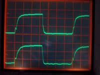
Although I have posted these photos in other thread, here they are. They are the new gate drive waveforms, using 6 ohms instead of 10 ohms.
I think the improvement is hardly noticeable.
In my opinion, the switching should be faster with this driver and the mosfets I am using (150V, 50 mohm, 3200pF máx Cin, 110nC máx gate charge).
I don't know what else can I do without using a buffer to improve rise/fall times, I will try to increase supply from 12v to 15v, and reduce freq. from 285KHz to, say, 230 KHz.
As before, waveforms are not time aligned, and lower trace is HS mosfet.
Attachments
Perhaps the IR2113 supply is not properly bypassed, because, basing on some numbers, rise and fall times should be in the order of 50ns for that current (2A) and mosfet caracteristics.
Perhaps I am not looking at the proper waveform. Is rise/fall time measured by looking at the Vgs waveform? If I look at the Vds waveform, switching time is about 50ns,that's right. But there is no great current flowing, so in the moment Vgs > Vth the mosfet is fully on, but when higher currents are flowing it won't be the same.
Any help?
Hi,
Yes it is the slew of the Vds you are attempting to speed up by speeding up the gate charging. In the period of that little blip you see on the gate signal just at the start of the rise, Vds switches in it's entirety. So you can bet it's switching fast! Drive beyond that point goes to ensure lowest possible RdsOn. This I believe is why speeding that up will aide further, but as stated already, it's all about finding that sweet spot, basically as fast as it can without becoming destructive due to the body diode.
Now, why wouldnt' the slew of the switching be the same with higher current?
PS still researching it but there's another good reason to use a follower, I just want to have some facts before I go posting about it. MOS outputs are far from ideal in a driver stage though.
Are these the gate voltages, right ?
The gate-voltage has in fact some indications on how a mosfet switches. But the actual output switching waveform and the gate input waveform are definitely NOT the same.
There are some good app notes on the switching behaviour of mosfets on the IR homepage.
The actual transition of the output voltage takes place where the input voltage shows this little step during its rise. This is where the driver has to "fight" against the miller effect of the gate-drain capacitance.
And yes: Proper bypassing of mosfet drivers is paramount.
And the mosfet you are using isn't an impossible load to drive, but an easy one it is neither.
Regards
Charles
Ok so the MOS outputs of the driver dont' have as constant an output impedance as a BJT buffer would, right? Or as low.
They're mosfets too they have to become well enchanced to get the lowest RdsOn as well this could help explain their sluggish drive.
I've seen people say ~300Khz is hard for these drivers to achieve, but I guess that'd depend on their load as well.
They're mosfets too they have to become well enchanced to get the lowest RdsOn as well this could help explain their sluggish drive.
I've seen people say ~300Khz is hard for these drivers to achieve, but I guess that'd depend on their load as well.
Wow! Your response time is faster than my mosfets' ! ;-)
Well, in that case, judging by the glitches in the gates, the switching time is about 50-60ns. I will measure it again with a faster timescale, however.
I measured the driver supply voltage and it is quite clean, some spikes of about 0.5V at the transition moments, but nothing more.
Then I can consider the case almost closed. As a conclusion, we could put a couple of formulas to help calculating the switching and conduction losses:
Switching losses: Psw=2 * Vrms * Irms * Fsw * (Tr+Tf)
Conduction losses: Pc=Irms^2 * Rds(on)
Please correct this if something is wrong. Specially if a 2 or 1/2 is missing. I want to account for the losses of BOTH mosfets, and be able to calculate them as a function of output voltage and current (Vrms and Irms)
BTW: with the last improvements in feedback and the reduction of gate resistors I have noticed a subjective decrease in the noise level of the amp. You must glue the ear to the tweeter to hear it!
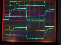
I am trying to calculate the actual dead-time basing on the gate waveforms. Let's see if I am doing this correctly:
Looking at one of the waveforms, for example HS (bottom trace):
I consider that the mosfets goes to ON just when there is a little peak in Vgs (entering in the Miller zone). This happens at about 3.5V (Vth). I consider also that the mosfet goes OFF when the falling edge crosses this level (Vth) again.
The period of the waveform is then T=3.45us (289.9KHz). The off time measures 1.835us, while T/2 should be 3.45/2=1.725uS.
So the dead-time is the excess of time that the mosfet is off, that is, 1.835us - 1.725us=110ns.
So I suppose I can go to a lower dead-time, say, 60ns safely, and this should reduce THD + N further.
BTW: I suppose that dead-time is also reducing the maximum modulation index: in this case, it is 6% of the period, so I can go up to 93% modulation. This explains why I only get 75Vpp while using +/-40V rails (measured at that load)! It was strange to me as Rds(on) should produce about 0.5V drop only.
In the figure I have drawn the timing I am considering.
Am I doing something bad?
Thanks!
Attachments
The period of the waveform is then T=3.45us (289.9KHz). The off time measures 1.835us, while T/2 should be 3.45/2=1.725uS.
hm, I suppose you did this with a grounded input and expected a perfect 50% duty cycle right?
What about the other factors that come into play though? Component delays, offset voltages etc. Assuming there should be a perfect 50% duty is a big leap to get your dead time from.
I think the only real way to get a working estimate of dead time is to measure the gate signals with respect to one another, and even that is hardly exact.
I also don't think it's possible to get such a tight dead time, it wouldn't take into account things like temperature variations, Vth is temp dependant.
The best you could do is use some sort of adaptive delay, and even that isn't ideal.
As far as max modulation goes, how is that for a good argument for going self oscillating? 😉
Regards,
chris
Yesterday I discovered a nasty problem with my feedback.
All had been going (surprisingly) perfect with my test loads. BUT as soon as I connected a speaker (yes, I couldn't help doing that ;-), the amp started to oscillate heavily.
The oscillation measures 71KHz, about 60Vpp and happens only with my speaker (a cheap 3-way bass reflex). If I connect a resistive load in parallel (say, 5 ohms), everything starts ok.
If I use only a 10 ohm power resistor, everything is ok too.
Then I believe the amp is oscillating due to the non-resistive impedance of the speaker. So I put hands into simulation again, modelled the speaker as 8 ohm in series with 1milliH, and was happy to found that with the same component values I can reproduce that oscillation quite accurately (although I change the speaker's inductance the freq. is the same).
I tested the phase margin and found that, in fact, it was going negative so everything matches. I had changed the resistor in series with the integrator capacitor to 1k, and that was a mistake: if I put 10K, the simulations go perfect and the phase margin, with that load, becomes about 33 deg.
The feedback components are:
- 10k series NFB resistor
- 68k || 68 pF comp. network
- 330pF + 1k (now 10k) integrator, in parallel with 150kohm
- 2k input resistor
Although I am almost sure that the change will improve things in reality too, I am now worried about when can I be sure that the amp will be stable for any speaker out there, what conditions should I meet and what a proper model should I use for my simulations of the speaker.
Charles, your help is particullarly helpful in these issues!
I have managed to put it to work with a speaker.
My simulation model has helped me a lot, as I have been able to measure phase margin and it was 0 or negative with the 1K resistor in series with the integrator cap as soon as the load became not purely resistive. As soon as I have increased it to 10K it is fine now.
The sound is fantastic and it starts reliably.
BUT (there is always a but :-( ), I have noticed that, with my 5 ohm test power resistor, there appear some oscillation (about 4vpp) superimposed to the signal when it is about to reach clipping.
The square wave response is fantastic, fast but no overshoot.
This phenomena has been more or less present during all my tests, and I don't know what it is due to.
I cannot reproduce that in the simulations, indeed the phase margin shown in it with this load is about 76 degs. Can you figure out what it is the cause?
This is the open loop response:
Attachments

BUT (there is always a but :-( ), I have noticed that, with my 5 ohm test power resistor, there appear some oscillation (about 4vpp) superimposed to the signal when it is about to reach clipping.
Can you post a screenshot ? What frequency approx is this oscillation ?
As to the load stability and loads for testing:
I don't know what I should say to this. There was once a standard dummy load for the testing of amps. It was part of the IHF A202 standard.
It consists of the parallel connection of a 12.6 mH inductor, an 800 uF cap and an 18.5 Ohms resistor. This is all connected in series with a 5.4 Ohm resistor. This arrangement emulates the behaviour of a woofer in a closed box, i.e. it is valid only for the low-frequency range where class-d amps excel anyway. There is obviously no standard describing stability requirements for amps at high frequencies.
OTOH there are amps out there that don't have any problems with some uF of pure (!!) capacitance connected to them (I remeber having witnessed how new receivers were tested at Revox, during quality control, by supplying full output swing at 15 kHz into 5 uF approx for about half an hour) while others have problems with a few nF of parasitic speaker cable capacitance.
I by myself am content if an amp is stable into resistive loads between 1 Ohms and idle (i.e. open output) and between 0.5 and 1 uF parallel to the nominal resistive load. That does not necessarily mean that it performs as well into all of these loads, since the capacitive load is detrimental to phase-marging (and therefore overshoot etc) and also frequency response (although this is corrected by NFB to some extent but it will still be detrimental to power bandwidth and therefore TIM as well).
And don't forget that one might be producing an amp that is stable into whatever load he could imagine and one fine day there comes the odd user connecting something really weird to it !
BTW: Do you still use a Zobel ?
I hope that all this was of some help.
Regards
Charles
Thanks, Charles.
Of course you are helpful.
About stability: I have simulated that "standard" speaker and the output is perfect, and the phase margin in the simulation is still above 73 degs.
Connecting a 1uF as the only load leaves a phase margin of only 25 degs, and some ringing in the pulse response, but as soon as the nominal load is paralleled (4 ohms, for example, PM becomes 49 degs, and everything looks perfect.
Now I have to test that in real life, as well as the no-load condition and capacitive loading.
And yes, I use a 22ohm + 120n Zobel network.
So in that aspect, I am quite happy with the results.
Now I have to fix the oscillation problem. I have to measure its frequency and perhaps take some screenshoots to post. Its frequency is not too high, perhaps the damn 70 KHz, so I think it's not RF noise from the parasitics.
Thanks,
Pierre
Now I have to test that in real life, as well as the no-load condition and capacitive loading.
Don't forget to wear protective goggles and a hard hat ! 😉
Regards
Charles
Thanks for the advice, Charles! 😉
About the ringing in the wave peaks, is there any particular measurement or test I can do to throw some more light on the issue? I say this because this afternoon I will have time for that, and I plan to take captures, for several loads (2.65, 5, 10 ohms), and measure its frequency.
I will also try adding more bypass to the bootstrap capacitor and see how it affects.
Best regards,
Pierre
- Status
- Not open for further replies.
- Home
- Amplifiers
- Class D
- Help with feedback