ok! thanks. (I just thought you were going to give me an idea, not that you were going to do calculations!)
Best regards
Best regards
I have increased the frequency and indeed the oscillation problem almost disappears. (only some near clipping peaks, but perhaps that's caused by missing pulses, not by inestabilities). This reinforces the theory that the problem was caused by violation of Nyquist theorem.
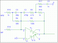
But as I don't want to go as high as 400KHz, I have tried to reduce the 0dB openloop point while keeping the original Fsw. I have done this by lowering the zero capacitor from 68pF to 33pF. This way I have been able to go back to about 280KHz with the same results.
I have also connected my damn speaker, and it doesn't make my amp a 200W oscillator and starts ok (if you remember I had that problem before).
However, I am curious to hear from Charles, both his opinion on this phenomena and also his other solution requiring a fast error opamp.
Best regards,
Pierre
Salut Pierre
Almost forgot you! The trick is a simple one: By putting a lag filter into the feedback path of the "integrator" (instead of the simple series resistor) you can generate some more phase-lead without adding another op-amp.
This does not need a VERY fast op-amp per se, but IMO at least the one that you originally used was a little "sluggish". Your amp circuit (partially due to your high triangle voltage) uses almost half of its published slew-rate capability. If you now take into consideration that the published slew-rate often applies for small-signal usage ...........
I haven't derived the exact formulae for the determination of thîs feedback circuit's component values yet. But one can always play around with values on a simulator ......
Regards
Charles
Attachments
A lot of thanks, Charles
!
The first simulation does seem to improve phase margin. I will try it because my second amp still has some ringing, although the components are just the same as the first one. I have also tried with a much faster error comparator and it shows no improvement.
Do you think that I can improve something by lowering the triangle amplitude to, say, half of the current value (6Vpp)?
I have also found a nasty problem again: when I was trying, suddenly the mosfets got shorted, so I have changed them. I am worried about that, because there was no apparent cause: no big power, not very high voltage (+/-45V), a 5 ohm load...
Does the failure mode (source and drain get shorted) tell something about the possible cause?
Best regards,
Pierre
This morning I have been doing some listening tests with both boards and a pair of big speakers (2x15" + tweeter each). The sound is impressive and amazing, although I have only tested at 200W peak power.
Suddenly, one of the boards (the last build) had blown the mosfets. They weren't hot, and both of them have become shorted. I have experimented this failure mode two or three times, and am very worried about it. In fact, the other amplifier has been running for quite a while and higher volume after that with no failure.
Is there a way to tell where the problem is coming? I assume that one of the mosfet fails, the other fails due to overcurrent in the next switching cycle (it tries to showt + and - rails). Unfortunately, the fuses are always much slower than the mosfets and don't save them.
If the gate is the problem, I assume that a 15V zener between gate and source should cure it, right?
If not, can the coil be the problem? They are wound on the same core, but the failed one has thicker wire and hence is wound less tight to it. But this failure has occurred also with a Wilco drum core, so I wouldn't suspect of the coil.
Does anyone have experience with this problem?
Thanks!
Hi Pierre,
Since they aren't running hot, I suspect a suddent death brought on by false turn on caused by Cdv/dt induced turn on.
I think any other possibility would lead to high temps and you'd know, like improper timing of the signals etc.
What happens is the slew across the mosfet gets coupled to the gate through the miller capacitance, charges up the gate-source capacitor and hits Vth, mosfet turns on when it's supposed to be off.... instant death.
So it's curious that one works while the other doesn't, I assume you kept all the trusted parts that worked before, but layout changed, maybe you have more inductance in the driver to fet loops this time around. Inductance in the source path is critical, I'm picturing Cdv/Dt bouncing off the source inductance like a spring hitting Vth.
Maybe a bypass cap or two would be a cheap fix but a decent test to see if it goes away.... it's a layout problem.
http://www.4qd.co.uk/serv/MOSFETfail.html#aval
Link talks about a few failure methods and causes, somewhat relevant.
It seems most failures are brought on by heat (with a few different underlying causes, but the heat is what kills them), Cdv/dt and avalanche seem to be two causes that may not heat it first.
Regarding the prior post, they always fail closed, all three pins shorted, it's very uninformative, other than to say you usually require a driver replacement as well.
Hope that's some help in some small way.
Regards,
Chris
Speaking of driver replacement, one way to prevent driver failure on experimental circuits is to buffer it with an IRF7343 set up as a source follower. It has protected my IR211x drivers every time so far.
Hello again,
Maybe the changed inductor can be enough to push it over edge too... complicated stuff 🙂
Here's a few papers I thought I'd share, they seem to discuss mosfet failure modes extensively.
See section 11 on page 24 for of this one for instance:
http://www.web-ee.com/primers/files/WebEE/AN-9010b.pdf
The quickest/not very scientific test here would be, try it with the inductor that you know doesn't cause any harm.
Here's another good one, about everything that is avalanche.
http://www.semiconductors.philips.com/acrobat_download/applicationnotes/AN10273_1.pdf
Two "keepers" for my collection of app notes.
Sub, thanks for that tip I'll check that part out.
Regards
Thanks for your help.
However, when this has happenede before, my driver hasn't failed.
BTW: both boards share the very same layout.
I'll look at it and tell you how it goes,
Pierre
However, when this has happenede before, my driver hasn't failed.
BTW: both boards share the very same layout.
I'll look at it and tell you how it goes,
Pierre
oppps. One moment, there IS a difference between both boards: the one that survives has a 0.05 ohms resistor between LS source and GND. I suppose that doesn't limit the shootthrough current too much (1800A at +/-45V!), but perhaps has an influence in the source path of the LS mosfet that helps damping things a bit???
BTW: classd4sure, about that fix you propose, how should I connect that bypass capacitors?
BTW: classd4sure, about that fix you propose, how should I connect that bypass capacitors?
Hmmm, .05ohm sounds like nothing huh, if you think about it though, source pin inductance is in the low nano realm, so it would like have a significant affect.
I trust that resistor isn't in the loop of the driver though is it? Damn, it's too bad Spice is junk for this sort of thing!
What kind of bypassing do you currently have, can we see a schematic of the driver section?
Throwing a few caps in there might do more harm than good so I'm reluctant to guess. Originally I was thinking if you had say, too big a ground loop from the driver to the source pin, a small cap from the source directly to the proper driver pin (ground or source reference) might help.
Chris, you're welcome. The IRF7343 has V(th) of only about 1 volt per MOSFET in its dual N/P package. An emitter follower buffer has a .7v Vbe drop--pretty close. Emitter followers are good, though, if the input drive is not enough to quickly switch the dual MOSFET.
Pierre, I am glad your MOSFET drivers are not blowing. When I used to blow a lot more MOSFETs, the reason was apparently linked to excessive dV/dt on the drains. Before I had found a way lessen current spikes more efficiently, I got around the problem with the use of a .5 ohm resistor placed in series with the transformer the MOSFETs were driving.
Pierre, I am glad your MOSFET drivers are not blowing. When I used to blow a lot more MOSFETs, the reason was apparently linked to excessive dV/dt on the drains. Before I had found a way lessen current spikes more efficiently, I got around the problem with the use of a .5 ohm resistor placed in series with the transformer the MOSFETs were driving.
Ooops again. The 0.05 ohms resistor is mounted but shorted, so no effect. Anyway, it is outside the VGS loop (driver LO output is connected to gate via the gate resistor/parallel diode, and COM pin is connected to the upper leg of the current sense resistor, whose lower leg is connected to Vss.
I will arrange an schematic for you to see it.
Thanks
I will arrange an schematic for you to see it.
Thanks
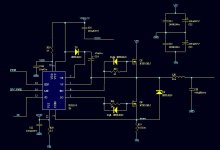
Here is an schematics of the power section.
The PWM and INV_PWM inputs have some deadtime, generated with the classical circuit (330R in antiparallel with a schottky, and a 33pF cap in parallel with each input pin). I took it from someone in the forum, ssanmor if I remember ok.
The rest is direct application of the IR2xxx datasheet.
If there is something weird, please tell me!
Thanks for your help
Attachments
Are you using output mosfets that are rated for reapplied dv/dt? I can't find a pdf for your mosfets, but maybe I've misread the part number (it appears to be NIP32N15). Mosfets weak in this regard may fail as you described. Note that IR parts are typically characterized for this parameter on the data sheet, whereas otherwise seemingly identical competing parts are not (they may be okay or may fail).Originally posted by Pierre This morning I have been doing some listening tests with both boards and a pair of big speakers (2x15" + tweeter each). The sound is impressive and amazing, although I have only tested at 200W peak power.
Suddenly, one of the boards (the last build) had blown the mosfets. They weren't hot, and both of them have become shorted. I have experimented this failure mode two or three times, and am very worried about it. In fact, the other amplifier has been running for quite a while and higher volume after that with no failure.
They are NTP35N15, from OnSemi.
What is the exact rating you are refering to and how do I calculate the acceptable value?
Thanks!
What is the exact rating you are refering to and how do I calculate the acceptable value?
Thanks!
I not only hunted down the right part number (couldn't tell from the schematic either), but the data sheet as well, neither was easy.
http://www.onsemi.com/pub/Collateral/NTP35N15-D.PDF
Pierre I just saw your post, I'll post this anyway because typing the name into search bar at onsemi didn't come up with anything.
I think we're going to get into an avalanche talk 🙂
If so that philips data sheet I linked to should be of some help.
Regards
Chris
Why do you think it's an avalanche issue? If so, how can it be corrected? (slower turn-on/off?)
Can false gate trigger be corrected by the resistor in parallel with Vgs that is often found in some designs?
Thanks for all your help
Can false gate trigger be corrected by the resistor in parallel with Vgs that is often found in some designs?
Thanks for all your help
OnSemi still does not rate its parts for this condition, I see (thanks for clarifying the part number, btw).Originally posted by Pierre They are NTP35N15, from OnSemi. What is the exact rating you are referring to and how do I calculate the acceptable value?
Years ago, just before they changed their name from Motorola, I tried some datasheet-perfect mosfets from this house that just would not work in class d. Look at the data sheet of almost any IR part (in the diode section) and you will see a rating for reapplied dv/dt (when the body diode had just been conducting). For older parts this limit was typically around 1 or 2 V/ns, but the newer parts are rated for as much as ten times that amount. The Motorola parts could only take about 10 V/us or so (much too slow for class d) when recovering into more than 40 percent of rated voltage at more than 5 to 10 percent of rated current.
Your OnSemi parts might do better than that (but who knows since they aren't rated), or maybe not. Since this is a secondary breakdown problem, it probably is most sensitive to voltage. The NTP35N15's are 150 volt parts so you might get into trouble with total voltages (both supplies plus spikes) of only 60 to 75 volts. If you can run the parts at full current with the supplies cranked down a bit, but get failures at only low to moderate currents with the supplies cranked up, then suspect a body diode reapplied dv/dt problem. If that is the case, the only cure is to change mosfet vendors.
- Status
- Not open for further replies.
- Home
- Amplifiers
- Class D
- Help with feedback