
Higher!?!about the class A bias, the original values of resistors are:
r30/r31, 0.47 ohm.
r6/r11 16Mohm.
what values shall I pick to make bias current a bit higher? I don't mind if it runs a little more hot, as I won't use it very often, just for learning and fun.
it seems some version of A1 just like on this schematic, it used
r30/r31 0.22ohm
r6/r11 3.7ohm
does this combination make bias current higher?
All the troubles comes from this amp being under dimensioned and with too little cooling for this high amount of Class A 😉
I highly doubt you'll be able to tell any difference if you actually turned the bias down .....

No worry about the cooling, I fine these little fan fit this amp very well.Higher!?!
All the troubles comes from this amp being under dimensioned and with too little cooling for this high amount of Class A 😉
I highly doubt you'll be able to tell any difference if you actually turned the bias down .....
With two of these inside, should keep it happy,
0.22 + 3.7m was not that ridiculous right? As it was in one version of A1, difference is ma50 has higher rail voltage, maybe make it a little bit hotter.
Maybe I can figure of the quiescent current by simulation, once I figure out how to set transistor parameters correctly.
I want to keep it around 0.7-0.8a, into 8ohm, thats about 8-10w class A, not too crazy right?
Attachments
It's easy to derive an approximate expression for the bias current.
From post #53, note the TR1 and TR2 base voltages are well matched and we'll assume equal base currents also. If R6 were open(0 current), the expected voltage at the right side of R24 is 0V, i.e. the input pair is perfectly balanced. Now considering R6 current and applying superposition, the expected voltage at the right side of R24 is 0V-(12V*R24/R6). Assuming perfect balance in the upper half, the output voltage will be 0V and the current through R30 will be 12*R24/(R6*R30). Plugging in actual values yields 12*47k/(3.7M*0.22) = 690mA. This is in nearly perfect agreement with measured current in reviews.
However in post 53, the voltage between TR9 and TR10 collectors is 0.101V, resistance between them is 0.44 ohm, so current is 230mA. Despite the discrepancy, I still have confidence in the analysis. It will be interesting to see what modeling predicts.
maybe just silly question, in your simulation, why don't you need to connect rail to power? it looks to me power not connected. sorry I am new to LTspice.When running the sim (if you are not that familiar with LTSpice, use the ALT key when hoovering over a component and select with left mouse key to see the power consumption in the component ... super cool feature)
PS. you need the BJT lib in same dir .. see zip file
you set the rail voltage to 12v? while its labeled as 20v.
simulation gave current through R30:It's easy to derive an approximate expression for the bias current.
From post #53, note the TR1 and TR2 base voltages are well matched and we'll assume equal base currents also. If R6 were open(0 current), the expected voltage at the right side of R24 is 0V, i.e. the input pair is perfectly balanced. Now considering R6 current and applying superposition, the expected voltage at the right side of R24 is 0V-(12V*R24/R6). Assuming perfect balance in the upper half, the output voltage will be 0V and the current through R30 will be 12*R24/(R6*R30). Plugging in actual values yields 12*47k/(3.7M*0.22) = 690mA. This is in nearly perfect agreement with measured current in reviews.
However in post 53, the voltage between TR9 and TR10 collectors is 0.101V, resistance between them is 0.44 ohm, so current is 230mA. Despite the discrepancy, I still have confidence in the analysis. It will be interesting to see what modeling predicts.
880ma for 3.7M*0.22
442ma for 3.7M*0.47
777ma for 1.8M*0.47
1.5a for 1.8M*0.22
204ma for 16M*0.47
16M*0.47 is my MA50 mono's original setting. Thats what? only 0.64 wats into 8ohm? that makes it almost pure class AB
this MA50 is initially advertised and sold as class A amp, unless I measured my r6, and r11 wrongly, they are actually cheating.
I measured these combinations because I have these transistors in hand.
In the simulation I can almost reproduce what happened on my amp by shorting tr1 and tr2 base, after they got shorted , these are the measurement:
r8: -622mv
tr1 base -636mv, emitter -68mv, collector -31.17v
tr2 base -636mv, emitter -68mv, collector -12.5v
tr9 collector -1.33v
r15 -11.2v
D9 and D10 are newly replaced, so it could be the pcb under D9 D10 is leaking?
r8: -622mv
tr1 base -636mv, emitter -68mv, collector -31.17v
tr2 base -636mv, emitter -68mv, collector -12.5v
tr9 collector -1.33v
r15 -11.2v
D9 and D10 are newly replaced, so it could be the pcb under D9 D10 is leaking?
It could be mere coincidence. Short bases in real life on the amp and see what happens. I doubt there'll be good correlation with simulation.In the simulation I can almost reproduce what happened on my amp by shorting tr1 and tr2 base, after they got shorted , these are the measurement:
r8: -622mv
tr1 base -636mv, emitter -68mv, collector -31.17v
tr2 base -636mv, emitter -68mv, collector -12.5v
tr9 collector -1.33v
r15 -11.2v
D9 and D10 are newly replaced, so it could be the pcb under D9 D10 is leaking?
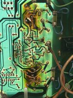
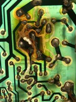
I get lost trying to find where the scorched areas are in the circuit, Is it inescapably clear that the burned spots are caused by the Zeners and their bias resistors? The 24 volt rails in the original schematic imply ZD1 and R13 each dissipate 0.3 W. This is way more than needed but is it enough to cause the damage observed?
Any thoughts about how to proceed this amp? I'd still like to help, but sure what to suggest without some guidance.
The practical options for repair have already been discussed. It's time to choose whether to make those repairs, assemble and fit replacement boards or quit fixing. You could offer the case and power supply to someone else who wanted to build with the available PCBs and get at least some cash for it.
As BSST mentions, the dark spots are are mostly due to overheating of the zener diodes and had they been located well clear of the PCB, the bad charring as well, may not have have occurred. The green dye used to colour the epoxy resin is very heat-sensitive and would darken eventually anyway, even as low as 45C internal temperature. It would not surprise me that this amplifier had been left powered up for days at a time and on several occasions either, so the problems may just have combined eventually into failure. At least there was no fire, which can happen when you operate these amps with the heatsink cover plates removed.
As BSST mentions, the dark spots are are mostly due to overheating of the zener diodes and had they been located well clear of the PCB, the bad charring as well, may not have have occurred. The green dye used to colour the epoxy resin is very heat-sensitive and would darken eventually anyway, even as low as 45C internal temperature. It would not surprise me that this amplifier had been left powered up for days at a time and on several occasions either, so the problems may just have combined eventually into failure. At least there was no fire, which can happen when you operate these amps with the heatsink cover plates removed.
Nicely spotted 🙂maybe just silly question, in your simulation, why don't you need to connect rail to power? it looks to me power not connected. sorry I am new to LTspice.
you set the rail voltage to 12v? while its labeled as 20v.
Yes late night mistake 🙂 ... just put it up to the rail values you are using ... is it 24V?
I am using 32v, but because I have a protection bulb in series with mains, the voltage is always much lowerNicely spotted 🙂
Yes late night mistake 🙂 ... just put it up to the rail values you are using ... is it 24V?
But anyway, the rail voltage is not quite relevant here.
How actually does it got connected in your schematic? I noticed the power rail is not physically connected to the power, but it still works, why?
Thanks, I just cant stopping chasing what is wrong here.The practical options for repair have already been discussed. It's time to choose whether to make those repairs, assemble and fit replacement boards or quit fixing. You could offer the case and power supply to someone else who wanted to build with the available PCBs and get at least some cash for it.
As BSST mentions, the dark spots are are mostly due to overheating of the zener diodes and had they been located well clear of the PCB, the bad charring as well, may not have have occurred. The green dye used to colour the epoxy resin is very heat-sensitive and would darken eventually anyway, even as low as 45C internal temperature. It would not surprise me that this amplifier had been left powered up for days at a time and on several occasions either, so the problems may just have combined eventually into failure. At least there was no fire, which can happen when you operate these amps with the heatsink cover plates removed.
But it looks like I am best off make a new pcb myself, shouldnt be too hard right? I am new to these stuff obviously
If the PCB is not burned/broken, then I do not think there is any reason for doing a new one ...... then it would be more fun to do a completely new and different amp.
Did you check the area I pointed out?
I attach an updated spice file, with correct voltages and the transistors you are using.
As for the Zenner, the issue here is that if it is mounted with the resistor value feeding it as used in the integrated amp, a lot of current (and a lot of unnecessary current) will flow through it. In the Integrated version the zenner regulator is also feeding the input section and therefore most of the current will flow in that direction and leave the diode with only a fraction (or at least much less) of current load. Also if the resistor value was not changed from the low voltage A1 version to the higher voltage version here (32V), then of course the current through the zenner will be even higher (don't know if this is the case).
For the MA50 you should only have a few mA flowing in the zenner. I would say 3 mA. If you use 4.7k for the resistor, instead of the 680 (or 470) ohm.
This will lower the zenner disipation to about 40mW and 85 mW for the resistor.
Attachments
If you reach the point that you feel the existing PCB is hopeless, a last resort would be to consider severing all traces passing through the burned areas and "air wiring" transistors, etc, as necessary. It would be ugly and tedious, but perhaps possible. Just another idea...
Spot on! Exactly what I would recommend, but I was thinking 3.3K. 🙂As for the Zenner, the issue here is that if it is mounted with the resistor value feeding it as used in the integrated amp, a lot of current (and a lot of unnecessary current) will flow through it. In the Integrated version the zenner regulator is also feeding the input section and therefore most of the current will flow in that direction and leave the diode with only a fraction (or at least much less) of current load. Also if the resistor value was not changed from the low voltage A1 version to the higher voltage version here (32V), then of course the current through the zenner will be even higher (don't know if this is the case).
For the MA50 you should only have a few mA flowing in the zenner. I would say 3 mA. If you use 4.7k for the resistor, instead of the 680 (or 470) ohm.
This will lower the zenner disipation to about 40mW and 85 mW for the resistor.
I completely agree with BSST. But first did yoy check that a trace has been burned through as someone asked prior?? That definitely looks like the trace has been damaged and should have a connection. Is there another to compare to, measure other with DMM for a short to both connection points. I have worked on a number of boards with carbonized portions that after parts replacement performed quite well. If you feel strongly that that might be it, then I would proceed with cutting traces out of the burned area and jumper in air as BSST has described. Don't have to do all of it, do one or two areas and see if it acts more like normal. I would do that before I start cutting and bondo ing.
What will be side affect if use 3.3k instead of 680? Or even 4.7k?If you reach the point that you feel the existing PCB is hopeless, a last resort would be to consider severing all traces passing through the burned areas and "air wiring" transistors, etc, as necessary. It would be ugly and tedious, but perhaps possible. Just another idea...
Spot on! Exactly what I would recommend, but I was thinking 3.3K. 🙂
I assumed 1mA bias needed by the amp, plus 5mA bias into the Zener, total 6mA. Assuming 20V across the resistor, 20V/6mA=~3.3K
Baldin elected a bit lower current in the Zener. Either should be fine and not produce so much destructive heat.
20V across 680 = 0.59W in the resistor and about 0.34W in the Zener.
Baldin elected a bit lower current in the Zener. Either should be fine and not produce so much destructive heat.
20V across 680 = 0.59W in the resistor and about 0.34W in the Zener.
Of course its been checked, not conductive, all obvious suspicions have been checked.If the PCB is not burned/broken, then I do not think there is any reason for doing a new one ...... then it would be more fun to do a completely new and different amp.
Did you check the area I pointed out?
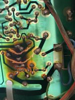
As people suggested, I carved the burned area as much as I can without completely remove and rebuild it. See pictures attached.
It seems improved a bit after that work, I am not 100% sure.
Now tr1 and tr2 emitter are around 480-500mv, about 100mv below ideal case.
Tr1 base still negative around -60mv, thats about 90mv below expected.
R15 is around -3.5v, thats about 1v below expected.
Rail voltage increased to 20v, with bulb attached.
Attachments
I also tested with bulb removed from mains.Of course its been checked, not conductive, all obvious suspicions have been checked.
As people suggested, I carved the burned area as much as I can without completely remove and rebuild it. See pictures attached.
It seems improved a bit after that work, I am not 100% sure.
Now tr1 and tr2 emitter are around 480-500mv, about 100mv below ideal case.
Tr1 base still negative around -60mv, thats about 90mv below expected.
R15 is around -3.5v, thats about 1v below expected.
Rail voltage increased to 20v, with bulb attached.
Rail voltage increased to 36.6v, thats a bit higher than I expected, I am using 120va transformer with 25vx2 outputs, maybe 36.6v is what I should expected?
With the rail voltage so high, three components runs hot:
Zd1, r13 and r19 as they all in much harder environment. Its not only this part, also apply to other channels.
Zd1 seems to struggle to pull the voltage down to 12.5v as I normally get. Its now 13.3v.
The transformer I am using now is new, but I think I replaced it as like for like. So 36.6v may be what it was running before. That should explain these burn marks on pcb.
It looks like I need higher power rating zd1, r13 and r19? Or increase the resistor values to say 4.7k r13 as people suggested earlier.
- Home
- Amplifiers
- Solid State
- Help please, Musical Fidelity A1/MA50 one channel distorted after about 10 seconds