Yes it does, again check everything around TR5, TR6, TR9 as mentioned above for issues. Go into pcb details! Double check this TR9.
Carbon track contamination is conducting ('burned') material unwanted, dragging the the system down.
When you sneeze upon the pcb, the amp goes beserk. Just imagine the unnamed conducting contends.
Yes, it is mainly carbon proper.
When you sneeze upon the pcb, the amp goes beserk. Just imagine the unnamed conducting contends.
Yes, it is mainly carbon proper.
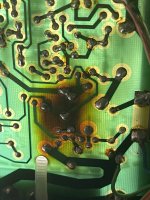
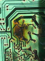
Carbonised circuit boards and most organic solids will be conductive to some extent, since they are effectively a charred mass of random high resistance tracks through the woven glass fibre fabric reinforcement here. Heavily carbonised materials such as PCBs made from phenolic or epoxy resin composites, can become highly conductive - virtually shorting from one track to another. Except that it means a complete rebuild of the board, a repairer should scrap a board like this and replace it if they expected to do a reliable repair. It may well have been cheaper to scrap and replace the whole amplifier in this case and for all we know, that could be how it came into your possession.
We DIYs being cheapskates of course, will prefer to dig out the darkened parts ourselves using a scalpel and mini grinder such as a Dremel tool then patch over the holes and gaps with epoxy filler compound. It's messy and ugly work but it can work if you prepare your board carefully, map out the existing traces and components carefully and replace any sections of copper trace that will be damaged or left unsupported, with solid wire links.
We DIYs being cheapskates of course, will prefer to dig out the darkened parts ourselves using a scalpel and mini grinder such as a Dremel tool then patch over the holes and gaps with epoxy filler compound. It's messy and ugly work but it can work if you prepare your board carefully, map out the existing traces and components carefully and replace any sections of copper trace that will be damaged or left unsupported, with solid wire links.
Last edited:

how do I find which part went conductive? Is it possible to detect it by using multimeter continuity test?Carbonised circuit boards and most organic solids will be conductive to some extent, since they have effectively burnt away to a mass of random high resistance carbon tracks through the woven glass fibre fabric reinforcement. Heavily carbonised materials such as PCBs made from phenolic or epoxy resin composites, can become highly conductive - virtually shorting from one track to another. Except that it means a complete rebuild of the board, a repairer should scrap a board like this and replace it if they expected to do a reliable repair. It may well have been cheaper to scrap and replace the whole amplifier in this case and for all we know, that could be how it came into your possession.
We DIYs being cheapskates of course, will prefer to dig out the darkened parts ourselves using a scalpel and mini grinder such as a Dremel tool then patch over the holes and gaps with epoxy filler compound. It's messy and ugly work but it can work if you prepare your board carefully, map out the existing traces and components carefully and replace any sections of copper trace that will be damaged or left unsupported, with solid wire links.
Tried for a while, didn’t find any place unexpected conductive. Also used alcohol and wipe to clean it.
not much change.
now it went back to bright bulb mode. so it’s intermittent
Also, can anyone explain to me why the abnormal voltage values have no bad effect on sound quality?
ever since c13 and c10 replaced, it has been sounded good despite what voltages are
ever since c13 and c10 replaced, it has been sounded good despite what voltages are
re:# 104
It needs a bit logic to see what the problem is. You can't really identify what parts are conductive until the board is stripped of components and connections. Any remaining resistances/shorts will still be elusive to identify until they are effectively isolated from all others. The more practical way to deal with that is just to attack the evidence, the darkened areas of board. Remove them completely and patch over, as described.
It needs a bit logic to see what the problem is. You can't really identify what parts are conductive until the board is stripped of components and connections. Any remaining resistances/shorts will still be elusive to identify until they are effectively isolated from all others. The more practical way to deal with that is just to attack the evidence, the darkened areas of board. Remove them completely and patch over, as described.
In that case, a new pub may be easier and cleaner. Plus can optimise the layout. The components are so crowed right now, make it so hard to work and test on.re:# 104
It needs a bit logic to see what the problem is. You can't really identify what parts are conductive until the board is stripped of components and connections. Any remaining resistances/shorts will still be elusive to identify until they are effectively isolated from all others. The more practical way to deal with that is just to attack the evidence, the darkened areas of board. Remove them completely and patch over, as described.
then the only thing can be reused from this is the chassis. Lol.
I read from this forum before someone said this amp is not worth to rebuild, now I understand why.
In that case, a new pub may be easier and cleaner. Plus can optimise the layout. The components are so crowed right now, make it so hard to work and test on.
then the only thing can be reused from this is the chassis. Lol.
You have just echoed my thoughts.
I assume there's no source of unpopulated PCBs? Do you feel up to creating a copy or a new board layout?
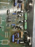
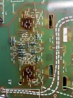
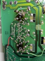
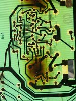
If it's not too much trouble, would you post close-up photos of the boards--- both top and foil sides? And particular details of the burned areas. Maybe that will spawn some ideas.
Well, original PCB copies and even completely different finished amplifier boards with modern output semis for A1 are available from China so you could explore those options at the usual online sources for no cost and, if you don't mind a little fiddling about to fit them to your case, you could proceed and wind up with something better again. I suggest that rebuilds are not often a simple thing to do properly, though. DIY can get very serious and be hell to troubleshoot when you screw up. That's right, screw-ups take up a large proportion of DIY time and why few of us ever make any income from it 
Here's an example of what you need for the royal road to repair: https://www.ebay.com.au/itm/2750114...39utmVOslaip6BVKsQtyaZ4wvJzSTci0aArazEALw_wcB
Just stumbled on this thread. Always good to see someone putting new life into old legendary products 
Looking at the schematics, I can´t understand why R13, R14 and ZD1, ZD2 should be so hot as to discolor the pcb?
Are they feeding other circuits not shown in the schematics on the first page?
According to the schematics they are only feeding the input stage!
I made a LTSpice sim file you can use ... need update on exact output transistors ...
Seems the amp is predominantly 3. order harmonic distortion, probably due to the high symmetry, decreasing the even harmonics
When running the sim (if you are not that familiar with LTSpice, use the ALT key when hoovering over a component and select with left mouse key to see the power consumption in the component ... super cool feature)
PS. you need the BJT lib in same dir .. see zip file
Attachments
I dont have experience to create a pcb before. Might not have time. But I am quite interested as the original board is low quality and obviously not optimal in terms of layout. They are lots of ways to optimise itYou have just echoed my thoughts.
I assume there's no source of unpopulated PCBs? Do you feel up to creating a copy or a new board layout?
If it's not too much trouble, would you post close-up photos of the boards--- both top and foil sides? And particular details of the burned areas. Maybe that will spawn some ideas.
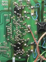
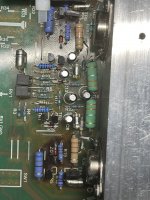
Here are the photos
Attachments
-
 7D5DFCFC-2B12-491A-A9F7-2BD0524D0118.jpeg505.4 KB · Views: 62
 -
 76E7C257-E43F-4786-9A12-0F0EA66B9E21.jpeg426 KB · Views: 55
 -
 1D03039C-3013-4C8D-BDE1-A0D70B4E8D4D.jpeg488.7 KB · Views: 56
 -
 97F4EF50-54C8-4FA6-AF8E-AF2E1D65F3DA.jpeg580.7 KB · Views: 55
 -
 0B11E937-AFDE-45A2-B8BD-50769E54EF44.jpeg497.2 KB · Views: 57
 -
 EF5C25A3-BB59-4AC3-975E-6545D1A6F22F.jpeg495 KB · Views: 51
 -
 4F3924FA-5164-45E1-8F68-44FD79A2A3FC.jpeg561 KB · Views: 58
I also have another board with almost all the components removed.(as its mono blocks, so comes as a pair) I didnt start to work on that one because stuck in this one
Here are photos of the other one
I dont know either why they got so hot, my other A1 model dont have these marks, but that was in lower power rail, +-24v, with 100va transformer, as shown on the schematic I posted
These zener diodes is not feeding anything else, because this is power amp version, there are no preamp section in it. In original A1 integrated version, one channel feeds two op-amps for line premap.
I read that this amp keep 2nd harmonic distortion by deliberately introducing dc offsets through r6 and r11, isnt that the case? I quite like the sound of this amp, for a small system of course. So picked this as my way step into the diy audio world.
Here are photos of the other one
Wow, just saw this, thats great. Where do you got these file from? You created them?Just stumbled on this thread. Always good to see someone putting new life into old legendary products
Looking at the schematics, I can´t understand why R13, R14 and ZD1, ZD2 should be so hot as to discolor the pcb?
Are they feeding other circuits not shown in the schematics on the first page?
According to the schematics they are only feeding the input stage!
I made a LTSpice sim file you can use ... need update on exact output transistors ...
Seems the amp is predominantly 3. order harmonic distortion, probably due to the high symmetry, decreasing the even harmonics
When running the sim (if you are not that familiar with LTSpice, use the ALT key when hoovering over a component and select with left mouse key to see the power consumption in the component ... super cool feature)
PS. you need the BJT lib in same dir .. see zip file
I dont know either why they got so hot, my other A1 model dont have these marks, but that was in lower power rail, +-24v, with 100va transformer, as shown on the schematic I posted
These zener diodes is not feeding anything else, because this is power amp version, there are no preamp section in it. In original A1 integrated version, one channel feeds two op-amps for line premap.
I read that this amp keep 2nd harmonic distortion by deliberately introducing dc offsets through r6 and r11, isnt that the case? I quite like the sound of this amp, for a small system of course. So picked this as my way step into the diy audio world.
Attachments

Trying it, I feel I jumped one level up in diy world in one day, lol.I made a LTSpice sim file you can use ... need update on exact output transistors ...
Seems the amp is predominantly 3. order harmonic distortion, probably due to the high symmetry, decreasing the even harmonics
When running the sim (if you are not that familiar with LTSpice, use the ALT key when hoovering over a component and select with left mouse key to see the power consumption in the component ... super cool feature)
PS. you need the BJT lib in same dir .. see zip file
how can I see the voltage on each component?
To someone might be of interest, here are a list of components I am using right now. The parts used are just cheaper ones. didn't pick low tolerant parts.
I will replace all the rest of resistors as well, a lot of old resistors seems to be in the signal path, I ordered some low tolerance parts from mouser.
c13, c14 will be replaced with bipolar caps
c10 will be replaced with film caps.
that basically will make this amp components completely new. Maybe its time to think about make a new pcb as well..... but haven't decided yet.
Attachments
about the class A bias, the original values of resistors are:
r30/r31, 0.47 ohm.
r6/r11 16Mohm.
what values shall I pick to make bias current a bit higher? I don't mind if it runs a little more hot, as I won't use it very often, just for learning and fun.
it seems some version of A1 just like on this schematic, it used
r30/r31 0.22ohm
r6/r11 3.7ohm
does this combination make bias current higher?
How do I update the transistor? the transistors I used is not in the list provided, and it doesn't allow me to customized a transistor: transistor properties sections are greyed out.I made a LTSpice sim file you can use ... need update on exact output transistors ...
Thanks, I saw this pcb on ebay as well.Here's an example of what you need for the royal road to repair: https://www.ebay.com.au/itm/2750114...39utmVOslaip6BVKsQtyaZ4wvJzSTci0aArazEALw_wcB
but a brief look at it can see many things not right, for example,
r24 is 1k and connected to r28 47k? that doesn't look right, and the size is not mimic the original. will make installation difficult.
also don't understand why it draw large transistor positions on PCB, they are super hot, impossible to be mount on PCB.
never mind, I figured it out. lolhow can I see the voltage on each component?
If you go to Mark Hennessey's site, you'll find there were many versions of A1 and many problems with reliability. However, it seems it was so popular that to satisfy ongoing demand, Musical Fidelity converted later designs to be somewhat similar but promoted them as A1 spinoffs, which to some degree, they were. https://www.markhennessy.co.uk/ Here is a quotation:
The MA50
This is a monoblock amplifier built into an A1 case, released in 1985. It's just an A1 with a bigger power supply - the PCB is the same, just the components relating to the pre-amp aren't fitted. Both power amp sections are fitted, and the outputs are wired in parallel. Apparently they are even less reliable than the A1!
,
- Home
- Amplifiers
- Solid State
- Help please, Musical Fidelity A1/MA50 one channel distorted after about 10 seconds