TR1 is leaking from base to collector: replace.
Voltage drop over R21 (top side) is 0.7V, 0.32 mA through TR3.
Voltage drop over R18 (bottom side) is 2.5V, 1,14mA from TR1.
Maximum current from R5 is 0.53mA, so the rest 0.61mA comes from R8 and D9.
Voltage drop over R21 (top side) is 0.7V, 0.32 mA through TR3.
Voltage drop over R18 (bottom side) is 2.5V, 1,14mA from TR1.
Maximum current from R5 is 0.53mA, so the rest 0.61mA comes from R8 and D9.
In the working amp, try changing R6 and R11 from 3.7M to 22M. I think the the amp will get less hot. Maybe then you can get some measurement without meltdown. We'll come back to the other channel and its problems.
Does the design author claim this is a Class A design? Does he have write-up of his design?
Does the design author claim this is a Class A design? Does he have write-up of his design?
Replaced tr1, no luck, things got a bit worse,TR1 is leaking from base to collector: replace.
Voltage drop over R21 (top side) is 0.7V, 0.32 mA through TR3.
Voltage drop over R18 (bottom side) is 2.5V, 1,14mA from TR1.
Maximum current from R5 is 0.53mA, so the rest 0.61mA comes from R8 and D9.
the voltage of tr1 base went up to -2.6v( it keep dropping), collector -8.3v , emitter -2.2v;
r8 -2.5v
tr2 base -2.5v, collector -8.5v
R5 up end 9v, bottom end -2.2v,
R15, -6v.
Tr9 collection -3.0v
Bulb is much brighter, while rail voltage dropped to +-9v. Which, I guess means the current in the amp is much bigger.
tr1 and tr2 has been replaced yesterday, and I noticed similar behaviour, that’s internal voltage goes up, rail voltage drop. I also noticed the rail will climb slowly, if I power on the amp longer and longer. meanwhile internal voltage drop.
is there kind of break in of new transistor going on?
Attachments
Last edited:
R26 is 1%, I replaced it.What is resistor tolerance of R22,R23,R25,R26? 5%?
R22,r23, r25, I don’t know, they are original
this circuit is designed by Tim De Paravicini, for Musical Fidelity in early years. It’s not pure class A obviously, but heavily biased to class A.In the working amp, try changing R6 and R11 from 3.7M to 22M. I think the the amp will get less hot. Maybe then you can get some measurement without meltdown. We'll come back to the other channel and its problems.
Does the design author claim this is a Class A design? Does he have write-up of his design
more detail can be found here:
https://www.markhennessy.co.uk/mf_a1/index.htm
I am working on model ma50, which is basically an A1 without preamp.
don’t have large resistors at the moment, will try later if I got any

I'm baffled. And wrong in this.Replaced tr1, no luck, things got a bit worse,
Bulb is brighter because much more current flows through TR9, lifted by TR6, lifted by TR5, lifted by more current through R18.
Where does this current comes from? Is TR5 not ok?
Intriguing and annoying!
With this split feedback loop, taken from the small dc voltages from R31 and R30, a dc- and temperature stabilisation is realised.Does the design author claim this is a Class A design? Does he have write-up of his design?
Unusual indeed, together with the reversed triple darlington outputs.
I have 1 tr5 damaged earlier before I posted this topic. But this new tr5 looks ok right now, and measured ok with multimeterI'm baffled. And wrong in this.
Bulb is brighter because much more current flows through TR9, lifted by TR6, lifted by TR5, lifted by more current through R18.
Where does this current comes from? Is TR5 not ok?
Intriguing and annoying!
how can a replacement of tr1 boost current so much? They are the transistor from the same batch, and the same has been used in the other channel, and another one of my A1 amp, don’t think it’s the new transistor problem.
despite the voltage and current goes completely wrong, it sounded still good, except noticeably louder background hum noise
despite the voltage and current goes completely wrong, it sounded still good, except noticeably louder background hum noise
After a few power on/off while I was measurementing.Replaced tr1, no luck, things got a bit worse,
the voltage of tr1 base went up to -2.6v( it keep dropping), collector -8.3v , emitter -2.2v;
r8 -2.5v
tr2 base -2.5v, collector -8.5v
R5 up end 9v, bottom end -2.2v,
R15, -6v.
Tr9 collection -3.0v
Bulb is much brighter, while rail voltage dropped to +-9v. Which, I guess means the current in the amp is much bigger.
tr1 and tr2 has been replaced yesterday, and I noticed similar behaviour, that’s internal voltage goes up, rail voltage drop. I also noticed the rail will climb slowly, if I power on the amp longer and longer. meanwhile internal voltage drop.
is there kind of break in of new transistor going on?
rail voltage now +-8.26v
r8: -1.36v
tr1 base -1.4v emitter -800mv, collector -7.8v
tr2 base -1.1v collector -7.85v
R15 -5.8v
tr9 collector -1.2v
The feedback loop tries to correct things.the voltage of tr1 base went up to -2.6v( it keep dropping)
tr2 base -2.5v
R15, -6v.
Tr9 collection -3.0v
If the current through TR9 increases, TR2 will draw more current from R5 so less current flows through TR1 and less through R18, causing the triple darlington to decrease the current through TR9 (see my post above).
But the loop is not able (enough) to correct this.
Base of TR1 keeps dropping... through D10 (again, the same chap). C13 don't like to much negative voltage (-3.0V from collector TR9). It should have its negative leg towards TR2, same as C10. Or bipolars, even smaller value poly's are ok for testing now.
You can put two diodes in series (anode on base TR5, cathode on collector TR5 = negative rail) to prevent the bias current running out of control. It should stay well under 1.4V (compare voltage drop of 0.7V over R21 on positive rail).
Same reasoning with your new measurements.
TR5 replaced... don't have c and e swapped incidentally?
TR5 replaced... don't have c and e swapped incidentally?
Thats not possible. Its clear labeled on pcb and I double checked the connections.Same reasoning with your new measurements.
TR5 replaced... don't have c and e swapped incidentally?
Attachments
I am wondering if it could be caused by out of spec old R6 or R8?
Their resistance are relatively large, so cant measure them on pcb.
Other old resistors I measured on pcb, r22, r23, r17 measured good.
just found my soldering station stopped working as well….. so can’t check
Their resistance are relatively large, so cant measure them on pcb.
Other old resistors I measured on pcb, r22, r23, r17 measured good.
just found my soldering station stopped working as well….. so can’t check
Btw, can I replace 47uf aluminum electrolytic capacitors with 10uf film capacitors? So it’s bipolar.
bipolar aluminum electrolytic capacitors is hard to find
bipolar aluminum electrolytic capacitors is hard to find
If you feel you're not making any progress, I suggest the procedure below. The general idea is to take as much circuity out of play as possible so there's less uncertainty with what remains.
1. Lift one end of resistors R6 and R11 so these are out of circuit. At this point I would make a quick powered check to see if biasing becomes more sensible. Doubtful we'll be so lucky.
2. Solder temporary jumper wires across R16 and R21 and install a 1k resistor across the speaker terminals. These steps should place TR9 and TR10 in cutoff; any leakage will appear across the 1k load at speaker terminals. Further, both long-tail-pairs should be biased at 0V, both at input and output--- quasi balanced. Maybe it will be easier to to spot problems in the input pairs.
3. If all looks in order, I'd first address the bottom half of the amp since it's most mysterious. Leave the short across R21 in place, but remove the jumper across R16. Disconnect the ground end of the 1k load and instead connect it to the B+ rail. When we apply power, we now have the bottom half of the amp enabled, and the top half is simply a 1k resistor pull-up to B+. The output should bias to 0V. Of course, you can investigate the top half independently of the bottom with a similar procedure.
thanks a lot, that sounds the only feasible way of testing left for me. I will try it.If you feel you're not making any progress, I suggest the procedure below. The general idea is to take as much circuity out of play as possible so there's less uncertainty with what remains.
1. Lift one end of resistors R6 and R11 so these are out of circuit. At this point I would make a quick powered check to see if biasing becomes more sensible. Doubtful we'll be so lucky.
2. Solder temporary jumper wires across R16 and R21 and install a 1k resistor across the speaker terminals. These steps should place TR9 and TR10 in cutoff; any leakage will appear across the 1k load at speaker terminals. Further, both long-tail-pairs should be biased at 0V, both at input and output--- quasi balanced. Maybe it will be easier to to spot problems in the input pairs.
3. If all looks in order, I'd first address the bottom half of the amp since it's most mysterious. Leave the short across R21 in place, but remove the jumper across R16. Disconnect the ground end of the 1k load and instead connect it to the B+ rail. When we apply power, we now have the bottom half of the amp enabled, and the top half is simply a 1k resistor pull-up to B+. The output should bias to 0V. Of course, you can investigate the top half independently of the bottom with a similar procedure.
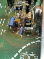
By saying R16 I think you mean r18 which is in parallel with c12?
And what is B+ rail? Is that the up positive power rail?
Yes, you are right. I misread the 8 as 6.By saying R16 I think you mean r18 which is in parallel with c12?
And what is B+ rail? Is that the up positive power rail?
B+ being the largest positive supply.
- Home
- Amplifiers
- Solid State
- Help please, Musical Fidelity A1/MA50 one channel distorted after about 10 seconds