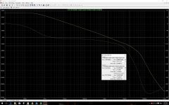
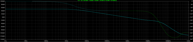
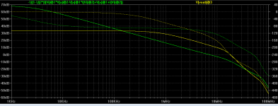
A stability question: I checked a closed loop bode with the version you sent, this is the 1st picture.
As I know with this -208° @ 0dB is not stable, right?
The closed loop phase response tells nothing, about the stability, especially if You include the input filter...
Sajti
Miller Compensation
Think there was an issue with the MIC inner loop. Here's another to try - Simple Miller. Not optimal by any stretch but think we're looking for stability at present. There is a little overshoot on square waves...
Think there was an issue with the MIC inner loop. Here's another to try - Simple Miller. Not optimal by any stretch but think we're looking for stability at present. There is a little overshoot on square waves...
Attachments
Last edited:
If you remove C4 (which grounds the output of back side of the LTP, and why?), that little overshoot will be gone. But simple Miller perhaps was not what the original design intended, as it came without degeneration at IPS LTP, and 470pF Miller cap would make a slow slew rate capability.
If you remove C4 (which grounds the output of back side of the LTP, and why?), that little overshoot will be gone. But simple Miller perhaps was not what the original design intended, as it came without degeneration at IPS LTP, and 470pF Miller cap would make a slow slew rate capability.
Maybe my sims are out but my analysis of the MIC loop didn't come out very well. What do you think? Have you had a go at simulating this amp?
The slew rate isn't good with 470p miller caps but still approx 20V/us. The LTP current is quite high (10mA) so that makes the miller caps look big initially.
Have to admit haven't got a lot of experience with this style of amp.
Paul
Yes, 20V/uS is what I meant slow.
I thought of trying it in LTspice but figured I'd better leave it to more experienced members. The original schematic seem to have lead-lag and multi path compensation that I feel above me.
Yes, 20V/uS is what I meant slow.
I thought of trying it in LTspice but figured I'd better leave it to more experienced members. The original schematic seem to have lead-lag and multi path compensation that I feel above me.
Could be wrong but i think the multi-path compensation was a product of desperation / confusion.
There are a lot of unknowns in this amplifier. The strategy I'm thinking of is getting it stable first by whatever means necessary then start to optimize for slew rate etc.
Think it is always advantageous to have many minds discussing a problem like this. Wouldn't say I'm an experienced member on this forum either. 🙂
There must be a simple way to compensate this amplifier... and have good performance.
Hi Guys!
Thanks for your simulations! I took a brief look to these versions of Paul
and I noticed an asymmetria: with this low impedance FB layout this 1G
DC FB isnt working right so the amp gets unbalanced!
I put back my DC servo (voltage source + 2k -> FB) and then its working again right.
I'll analyse them in more detail later tonight.
Thanks again for every idea, advice, tip on this challanging amp! 🙂
Hi Guys!
Thanks for your simulations! I took a brief look to these versions of Paul
and I noticed an asymmetria: with this low impedance FB layout this 1G
DC FB isnt working right so the amp gets unbalanced!
I put back my DC servo (voltage source + 2k -> FB) and then its working again right.
I'll analyse them in more detail later tonight.
Thanks again for every idea, advice, tip on this challanging amp! 🙂
Apologies again! You are correct the 1G cap wasn't supposed to be left there. So, yes, you are right, your simulated servo is fine. Grabbing time when I can this weekend....
Could be wrong but i think the multi-path compensation was a product of desperation / confusion.
There are a lot of unknowns in this amplifier. The strategy I'm thinking of is getting it stable first by whatever means necessary then start to optimize for slew rate etc.
Think it is always advantageous to have many minds discussing a problem like this. Wouldn't say I'm an experienced member on this forum either. 🙂
There must be a simple way to compensate this amplifier... and have good performance.
If we discard whatever the compensation scheme was with the original design and make it a simple Miller, your circuit is quite good. I disconnected the C4 and C5. The loop gain plot shows a 71-deg phase margin, and 25dB gain margin.
Attachments
If we discard whatever the compensation scheme was with the original design and make it a simple Miller, your circuit is quite good. I disconnected the C4 and C5. The loop gain plot shows a 71-deg phase margin, and 25dB gain margin.
Nice and simple. 🙂
If we increase the gain a little by changing the feedback shunt resistor from 1K5 to 1K we reduce the ULGF down to 1.1MHz and increase the phase margin to 81 degrees while gain margin stays at 25dB.
Seems reasonable to me to have a slightly higher gain due to the 60V rails. At the expense of a little feedback at 20KHz though.
Attachments
Nice and simple. 🙂
If we increase the gain a little by changing the feedback shunt resistor from 1K5 to 1K we reduce the ULGF down to 1.1MHz and increase the phase margin to 81 degrees while gain margin stays at 25dB.
Seems reasonable to me to have a slightly higher gain due to the 60V rails. At the expense of a little feedback at 20KHz though.
Right, we can do that too.
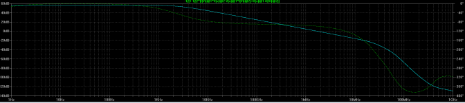
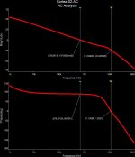
The next I'd do is to degenerate the IPS pair by factor of 10. So two 47-R resistor went in. Miller C reduced from 470pF to 68pF. The feed back shunt resistor is still 1k5 for gain of 23x. Caps across the driver transistors' B-C were reduced to 47pF. On the loop gain plot, both phase and gain margins are healthy, yet the speed of the amp has got a big boost. The simulated square wave response shows the amp is capable of 84V/uS transition at output.
Attachments
This is indeed a big step forwards. Hadn't realized the full benefits of IPS degeneration. A while back I was designing an amp and decided that it wasn't a benefit in that design. That's when it disappeared into the mists of time...
Two comments. I would prefer to keep the driver caps at 220pF and accept the small amount of stability loss. In my experience they needed that to keep stable. But 47pF may be OK in this amp. Also, still prefer the increased gain by changing the feedback resistor to 1K.
Should be interesting if Cortez implements these ideas!
Hi Guys!
First of all, thanks a lot for working with the circuit and my problem! 😉
My late night program streched a bit so I cant try it now but anyway I'll review your solutions in spice first.
I am also not familiar with this Tian method so I have to learn it as well.
First of all, thanks a lot for working with the circuit and my problem! 😉
My late night program streched a bit so I cant try it now but anyway I'll review your solutions in spice first.
I am also not familiar with this Tian method so I have to learn it as well.
Well then... I have a few questions:
I found an article about this Tian method and I'll read it tomorrow, but nattawa
am I right using your circuit I just have to run the simulation and add a trace
with that long formula you just put in the spice file as a comment on the top right?
If this is true, I played with this circuit and tried the following things:
I only know the theoretical basic rule about 0db < 180° but in practice whats the rule to be sure..?
Is this 3rd version still ok for example or on the edge..?
I just would like to have more different options and have alternatives I can try later in reality.
I found an article about this Tian method and I'll read it tomorrow, but nattawa
am I right using your circuit I just have to run the simulation and add a trace
with that long formula you just put in the spice file as a comment on the top right?
If this is true, I played with this circuit and tried the following things:
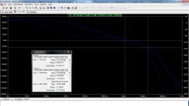
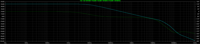
- note: image #1 shows this output, based on your setup.
- I tried going back to my original values and layout: FB Rs, DC servo (I hope it's not a problem)
and as I saw it didnt change the stability (but means a lot less work with my messy PCB... 🙂)
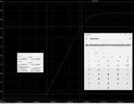
-> image #2 - then I tried Paul's method instead of the Miller cap with 2x10pF (from VAS PD/ND -> FB)
-> image #3
I only know the theoretical basic rule about 0db < 180° but in practice whats the rule to be sure..?
Is this 3rd version still ok for example or on the edge..?
I just would like to have more different options and have alternatives I can try later in reality.
Attachments
My version
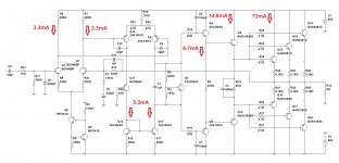
Hi Cortez,
Please see my version after some corrections.
Key points:
- your design is rather stressed in terms of the working points, I have reduced the standing currents to the appropriate (from my view) values.
- emitter degeneration and base stoppers; note 22R connected to ground.
- compensation is simple Miller plus a little bit of lead (1pF).
That's basically it.
TO-126 transistors and the drivers are slightly different - I just had the good models for the one I used - but that's ok, substitution is good enough.
Cheers,
Valery
P.S. Ah, one more thing - quality of differential cascades and current mirrors is much better if you use the same type of transistor for both shoulders 😉
Attachments
Last edited:
Wow Valery, first of all thanks a lot for your time and effort
(specially drawing my cicrcuit from scratch in your software..)! 🙂
Now I have 3 different versions to try so I'll ask for a bit of patience I hope no one is offended... 🙂
And I also accepct your critcism this is a partially experimental "design" even if
it's unbalanced as mentioned. Your version is almost a completely different amp now
which would be a real horror for me to adopt now with this crowded PCB I have.
Please also consider this amp was already working/singing and almost stable
but at some mystic circumstances it started to oscillate but as I was told
this can be easily caused just by these underhand drivers I am using now.
(They tend to oscillate just at a certain temperature + PS voltage level + load + time, etc...)
That's why I asked how to determine whether an oscillation is caused by just
some OPS issue or by improper compensation (or maybe both of them...)
Now I think I'll start to check and "merge" your versions and start from my actual one
and check in Spice with this Tian method whether it's worth a try in reality...
Wow Valery, first of all thanks a lot for your time and effort
(specially drawing my cicrcuit from scratch in your software..)! 🙂
Now I have 3 different versions to try so I'll ask for a bit of patience I hope no one is offended... 🙂
And I also accepct your critcism this is a partially experimental "design" even if
it's unbalanced as mentioned. Your version is almost a completely different amp now
which would be a real horror for me to adopt now with this crowded PCB I have.
Please also consider this amp was already working/singing and almost stable
but at some mystic circumstances it started to oscillate but as I was told
this can be easily caused just by these underhand drivers I am using now.
(They tend to oscillate just at a certain temperature + PS voltage level + load + time, etc...)
That's why I asked how to determine whether an oscillation is caused by just
some OPS issue or by improper compensation (or maybe both of them...)
Now I think I'll start to check and "merge" your versions and start from my actual one
and check in Spice with this Tian method whether it's worth a try in reality...
Exactly - that's what I was actually going to suggest - just use it as a guide with some ideas on how to make it stable.
Although, I would start with reducing the driver's quiescent current - 54mA in your original design looks way too much to me... TO220 will hardly survive 😉
Ok and thanks for your understanding! 🙂
About this Tian method nattawa showed me:
Is this formula and bode plot giving the final loop gain or "just" the open loop gain?
So how should I check the phase margin at 0dB or when it is crossing to the CL gain level..?
And what about the gain margin @ 180°: can someone give me a practically
good value that already can be accepted?
BTW: nowadays with these developing AI techniques I can imagine an evolution
algorithm kind of process where an ideal compensation can be achieved by CAD...
Last edited:
I found this article about the Tian method (for another simulator but the point is the same):
Plotting Loop Gain Using the Tian Method - Spring 2011
Based on that I suppose with this Tian formula the bode shows not the OL but the "loop gain".
And with this 3 steps trick mentioned it's easy to plot both the loop gain and the CL bode as well.
But I am not an LTSpice expert, specially when it comes to tricks like stepping and expressions...
Please review my solution, is it correct this way?
.step param prb list 1 2 3
AC amplitude of Vtian = {table(prb, 1,1, 2,0, 3,0)}
AC amplitude of Itian = {table(prb, 1,0, 2,1, 3,0)}
AC amplitude of Vin = {table(prb, 1,0, 2,0, 3,1)}
I'll now check the compensation based on this setup so please say quickly
if it's wrong, otherwise my afternoon will be just a waste of time... 🙂
Other thing: as Cordel didnt publish model for my NJW bjts are these MJL4281C/MJL4302C models
good substitutes or simulating with these can be easily lead me to some false consequences..?!
Attachments
........
Two comments. I would prefer to keep the driver caps at 220pF and accept the small amount of stability loss. In my experience they needed that to keep stable. But 47pF may be OK in this amp. Also, still prefer the increased gain by changing the feedback resistor to 1K.
Should be interesting if Cortez implements these ideas!
Understood. I suspect the caps at drivers B-C are more of physical implementation dependent, such as the PCB layout, wiring, power rail decoupling, transistor specifics, and other construction details, as the loop gain plot shows no significant change responding to their values between 47pF and 220pF. From my own limited experience I got away with no caps at driver transistors' B-C.
1K for a higher gain is a valid point for a 200W grade amp. However one must be pleased to know the same compensation design will work at lower supply voltages, lower output power, and lower gains and still be stable.🙂
- Status
- Not open for further replies.
- Home
- Amplifiers
- Solid State
- Heatsink vs OS stability