Absolutely.raise the bar a bit more
I want it to be more efficient and the "go to" design for
the power hungry. Without being a "boat anchor" 10 pair mt-200
Frankenstein.
I have simulations of the 2X/3X versions already to go.
Once I start layouts , no turning back.
PS - I am still researching class G/H. To truly temper a discussion
without subjectivity , I must get through all the "myths".
What is nice , this H experience is increasing my knowledge of AB ,
and vice versa.
OS
Last edited:
Raise the bar ??
The question is , is it still CLASS H .... ??
Noticed that the class H trackers were sharing current below
the switching threshold anyway.
Increased that effect all the way by turning the trackers into glorified
high current series regulators (cap multipliers , too).
Low level audio , the inner pairs are still on 20V supplies. High level
the current sourced reference tracks up to the 60 rails.
So , the inner/outer rails both always conduct , but the 20V low voltage power
supply is eliminated.
- Eliminated one whole power supply , and it's power use. Does this not
keep the class H efficiency ? Same power is just being used by the 60V supply.
- Having Vceo and I shared between outer/ inner pairs , do I still get the same
SOA advantages ??
No big switching dual Schottkey - it is gone.- Current/non-switching is better , as well. 20+ Khz is still non-switching - I like.
Still do not know what I have here ??
- Still need to learn MORE!
OS
Attachments
I have to admit that I still don't get what makes the outer devices oscillate?
Best regards!
Oscillate , when do they do that ??
They track the inner pairs , but don't oscillate on their own.
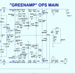
Outer pairs are CFP .. let me show you some real oscillation ....
- removed C111 , no bypass of Q110's Ccb. Hmmm , 20mhz "excited"
and enhanced by the clipping of the output stage. This is expected errata
from a CFP. With C111 , stable as all hell.
PS - I do think I still have class H here , even without the 20V supplies.
At 15V p-p , FR+/FR- are at a nearly regulated 21V inner/ outer would
dissipate FAR less heat at 20-40V Vceo , AB OPS's I have ran at <40V are
nearly cold with normal loads.
Inner pairs run at that regulated 21V not only have 30+ more DB of PSRR ,
But dissipate almost no heat.
Outer pairs NEVER see more than 39V Vceo , inner pairs see >39V only
when approaching the rails. I am almost sure I still have a "strange" class H
with all it's advantages.
PS - or "Class OS" 😀
OS
OS
Attachments

Last edited:
I interpret that in this way from pictures you'be been showing in #100 e.g.
Best regards!
Nope , outer output pair "tracks" the >21V excursions of the main audio
output waveform. (below 2). It just "copies" the main waveform + 4.7V.
When there is no demand for room shaking volume , the outer devices idle
and just series regulate a firm 21V for the inner pair to work from (below 1).
A "normal" Class H has a dedicated 20-(21V) supply for this "mode".
A normal OEM class H (and G) makes switching noise as the lower 20V supply
is disengaged and the higher modulated one "kicks" in. When this higher
supply kicks in for it's half cycle , the outer transistors also switch.
These standard class G/H traits are why "audiophiles" avoid this tech.
Pro applications just want gobs of power to fill auditoriums with $$$.
Purity is less of a concern to them.
Most also "average' the tracking , relying on the fact that the bass waveform
will be dominant in determining the waveshape.
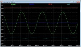
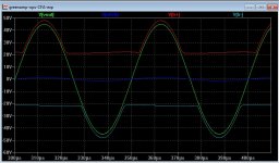
(below 3 ) I try to go "overkill" on both the switching and tracking.
Clipped waveform with unrealistic 100khz square wave. See if we remain
non-switching and can faithfully track (without any instability - below 3).
The GOAL is to have a 4 device 200W output stage that runs as cool
as a 60W one , now hopefully eliminating the complexity that this class
H entails. 30ppm THD 20k is another goal.
Edit - Kay , that "oscillation" is my 1K/100K "abuse' input waveform.
To test just a fundamental 10-20khz is not a realistic test.
This is how I get 99% from simulation to real amp success.
OS
Attachments

Last edited:

The question is , is it still CLASS H .... ??
Eliminated one whole power supply , and it's power use. Does this not keep the class H efficiency ?
No and no, unfortunately.
Best wishes
David
No and no, unfortunately.
Best wishes
David
Explain this.
If it is not using the 20v supply and using the 60v one , is it not using the same watts? One is just being swapped for the other.
How about the other class H advantage , do the inner/outer devices still
"share" SOA ?
Explain this.
...do the inner/outer devices still "share" SOA ?
Conservation of current, the load still sees the same current and it's all drawn from the 60 V supply.
Power = I x V.
For a Class H amp most of the current is drawn from the low volt supply, requires less power.
Yes, the devices still share, so you have reinvented the old "stacked" OPS, used in the early days of solid state when transistor's SOA was pretty poor.
Marshall Leach and the like IIRC.
Best wishes
David
It does however, let you use a fragile high frequency capable output transistor operating at low voltage to get single digit ppm distortion, leaving the heavy lifting to the slower, more rugged slave device(s) which can’t get that kind of performance on their own.
Replace the tracker with a device(s) operating in switch mode and you have the Yamaha EEEngine, or the basics of the Labgruppen FP series.
Replace the tracker with a device(s) operating in switch mode and you have the Yamaha EEEngine, or the basics of the Labgruppen FP series.
Conservation of current, the load still sees the same current and it's all drawn from the 60 V supply.
Power = I x V.
For a Class H amp most of the current is drawn from the low volt supply, requires less power.
Yes, the devices still share, so you have reinvented the old "stacked" OPS, used in the early days of solid state when transistor's SOA was pretty poor.
Marshall Leach and the like IIRC.
Best wishes
David
Got the first part , power is the same for the original Crest class H simulation with V1+3 - I ,
versus just the V1 - I of this design.
Why would the 20V supply (in isolation) use less power than the 60V one
through a series regulator set to the same 20V ??
I do know there is loss through the series regulator , but it is <100ma.
Class H's efficiency is dynamic , most of this efficiency is derived at the
low end ( under 20V) , and approaches class B as output increases.
So , "faking" the 20V with the class H tracker ,
you lose (some)efficiency through the thermal and circuit losses of the outer device.
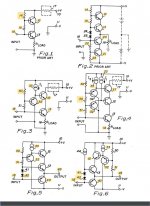
(below) is the patent for the "stacking". Fig. 6 is closest , but it is just
crude proportional - no setpoints (zener references.)
I agree we lose some of the class H efficiency , but not all of it.
Have to rethink the goals.
-I want a cooler amp , with cheaper heatsinks.
-I want to get better SOA out of cheap devices.
A "stacker" sounds nice. OEM's seem to want this , too. Crest uses a 1+KVA toroid with dual secondaries. Not a lot of efficiency. They use small heatsinks ,
economics to make use of the cooler , lower SOA.
OS
Attachments
Last edited:
Are you not going to sacrifice some efficiency to heat running from a single 60V supply?
Oh , hi Jeff.
Yeah , let me explain the problem. Typically < 20p-p music will use the
low supply only. high transistor and supply are off.
With my last change in design , the low supply was created from the high supply.
Current would always flow through all transistors. So , efficiency would be
lost through the heat lost by the high transistor.
But , would their combined heat be more than the heat from a single transistor running from the full 60V rail ?
I do know the heat would be more than a single transistor running the low 20V
rail. This class deals with the physics of the BJT semi junction , as far as
efficiency goes.
PS - short of a SMPS , ridding yourself of a whole supply would be
an (global) efficiency gain in itself.
OS
Last edited:
In your schematic the output transistors are pushing 11.5A with 2V Vce. This is where quasi-saturation can be a stumbling block.
I updated the 5200/1943 models with quasi-saturation curves from the Fairchild datasheet:
.MODEL FJP5200-O_kq npn ; by Keantoken - Feb 20 2019
+ Bf=130 VAF=400 CJC=380p TF=5n Ikf=70 CJE=6.1n IS=300f
+ NF=1 BR=8.025 NR=1.0 ISE=10p NE=2.0 ISC=2.01764E-10
+ NC=1.5 VAR=100 IKR=1.39087 RB=1.1 RBM=0.00011
+ IRB=1.51189E-6 RE=0.0032 VJE=0.711 MJE=0.304 FC=0.5
+ VJC=0.84 MJC=0.25 TR=3.342E-7 XTB=1.72 EG=0.78 XTI=3
+ Rc=0.1 Rco=.56 Gamma=30n Vo=22 Nk=.9
+ Vceo=230 Icrating=15A mfg=Fairchild
.MODEL FJP1943-O_kq pnp ; by Keantoken - Feb 20 2019
+ Bf=112 Vaf=80 CJC=750p TF=5n Ikf=6.5 CJE=5.26n IS=650f
+ NF=1 BR=8.805 NR=1.0 ISE=10p NE=2.0 ISC=2.01764E-10
+ NC=1.5 VAR=100 IKR=1.39087 RB=1.1 RBM=0.00011
+ IRB=1.51189E-9 RE=0.0061 VJE=0.711 MJE=0.304 FC=0.5
+ VJC=0.84 MJC=0.25 TR=3.342E-7 XTB=2.28 EG=0.81 XTI=3
+ Rc=0.05 Rco=.22 Gamma=800p Vo=12 Nk=.53
+ Vceo=230 Icrating=15A mfg=Fairchild
Last edited:
In your schematic the output transistors are pushing 11.5A with 2V Vce. This is where quasi-saturation can be a stumbling block.
I updated the 5200/1943 models with quasi-saturation curves from the Fairchild datasheet:
They work , thanks. I notice 4R loads show worse (maybe more realistic)
THD. That is up at the >10A range.
OS
In your schematic the output transistors are [near] quasi-saturation...
Also the Baxandall super pair transistors in the VAS/TIS of course.
I know you have looked at this and done models, I was just about to PM you and ask for comments so I could improve my own models for low power transistors.
So your post is timely, any advice?
Best wishes
David
Also the Baxandall super pair transistors in the VAS/TIS of course.
It's important not to assume, and look up the datasheet. The BC5xx have virtually no quasi-saturation behavior or traces of Vce breakdown (compared to common VAS transistors). In fact they are so perfect that they are actually worse for a VAS because there is no gradual Vce breakover to compensate for the increasing voltage gain as Vce increases.
Also, the NEC datasheets for the 2SC1845/A992 show significant quasi-saturation and the Fairchild KSC/KSA datasheets are just shameless copies of the same graphs. But if you measure the Fairchild devices the quasi-saturation is gone. So I guess, there be dragons.
I know you have looked at this and done models, I was just about to PM you and ask for comments so I could improve my own models for low power transistors.
So your post is timely, any advice?
Best wishes
David
Well without an object of critique, I can only guess at the deficiencies, but assuming you are up to date on SGP modeling, here is what I think is on the frontier with VBIC models:
Installing and using ngspice - an opensource simulator
It's important not to assume, and look up the datasheet. The BC5xx have virtually no quasi-saturation behavior or traces of Vce breakdown (compared to common VAS transistors)
I didn't assume that the Baxandall super pair is near saturation, it demonstrably is (well, the one that makes it a super pair)
I remember that the BC5xx are pretty nice for quasi-saturation, I planned to use them for the saturated transistor in the pair if I ever use that circuit.
Well without an object of critique...
I didn't expect you to do my homework😉
Just some comments on the process, which order to do parameters to minimize interactions and so on, like Bob Cordell discusses in his book.
Thanks for the reference, I'l look at it.
Best wishes
David
Last edited:
- Status
- Not open for further replies.
- Home
- Amplifiers
- Solid State
- GreenAmp ++ modulated Class G output