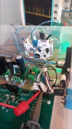
Some pictures of the connections....
//
Does it help when you run ground wires in the bundles of digital signal lines, straight to SV1 and SV2 pins 1 and 3?
Doing a functional test here is more difficult than I thought; I have something that can generate a sigma-delta modulate and wck, but no mck. I have to think about it, maybe I can check something at half speed.
Last edited:
Thanks - I'll try that!
I suppose you mean ground from EVM and also the Ian board...to SV1 and SV2?
//
I suppose you mean ground from EVM and also the Ian board...to SV1 and SV2?
//
Yes, EVM ground to SV2 ground and SV1 ground to the Ian board ground (in order to keep the loop areas of the digital signals and their ground returns small, as far as possible).
Did grounding. No big change.
Observations:
At power on, after a few seconds a (1) green LED is lit in the Mojo.
Probing the BCK, it looks weird - more like data than a clock. Like what I sent before.
When lifting the probe to the other i2s pins a few times back and forth, the LED goes out and BCK disappears.
//
Observations:
At power on, after a few seconds a (1) green LED is lit in the Mojo.
Probing the BCK, it looks weird - more like data than a clock. Like what I sent before.
When lifting the probe to the other i2s pins a few times back and forth, the LED goes out and BCK disappears.
//
It could also be that the EVM clocks need to be running before the FPGA board is powered up.
Pity that the extra ground wires didn't help.
If the green LED is LED9, then it's supposed to light up until 1.365333... seconds after the end of the clipping event whenever the FPGA detects that something is clipping.
Pity that the extra ground wires didn't help.
If the green LED is LED9, then it's supposed to light up until 1.365333... seconds after the end of the clipping event whenever the FPGA detects that something is clipping.
Last edited:
You see it in #439 - its the one in the end of the line of LEDs near the reset button so could be LED9 - I cant find a layout that defines the position of the LEDs. Probably is... So that one should not be lit the whole time? It is now... But I have seen it go out on occasion... I thought you did use a special pin to drive a LED (that I needed to supply and connect) at clipping and not one of the 8 green "board residential" ones...
I'll try a phased power-on...
//
I'll try a phased power-on...
//
Btw, I'm back at the China i2s/opto board as Ian informed me that I could not use only the Interface board but also needed a FIFO board to get that going... I cant fit that into the box so... But I think if we can get the Mojo to start without being in constant clip and also a Data that doesn't look like a clock, maybe it turns out that we get a good s/pdif...
What should i2s Data really look like?
//
What should i2s Data really look like?
//
Could you make a single-shot scope plot with both MOD6 and MOD5 in it? If the EVM produces two's complement while my filter expects offset binary, it will always clip except in the peaks of extremely loud sounds.
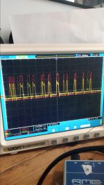
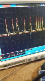
Here goes. There was no Mic connected as I have to look at it while making the second one.
//
Do you mean that the analogue inputs of the EVM were open? Or that the EM273 was disconnected, but the OPA1612 and the rest was still connected?
I don't understand the amplitude difference, but when MOD5 and MOD6 move in phase during silence, it's probably two's complement rather than offset binary. I then have to remove an inverter and resynthesize the configuration file.
Could the modulator output with the small swing be shorted to some quiet digital output? When two digital outputs are shorted and one tries to drive the line low and the other tries to drive it high, you get some intermediate voltage (or smoke, depending on how strong the outputs are).
Attached is the two's complement version, as usual you only need the .bin file. I've checked that I could program it into my FPGA module with Mojo Loader. The progress indicator worked and in the end the program said that programming and verification were "Done". The red LED turned off at the start of programming and back on again after verification.
There are two changes, the change from offset binary to two's complement and a corrected CLKIN_PERIOD value for the DCM. According to Xilinx, having a wrong CLKIN_PERIOD either has no effect at all or only leads to a small increase of the clock jitter, so it doesn't explain the problems you have.
There are two changes, the change from offset binary to two's complement and a corrected CLKIN_PERIOD value for the DCM. According to Xilinx, having a wrong CLKIN_PERIOD either has no effect at all or only leads to a small increase of the clock jitter, so it doesn't explain the problems you have.
Attachments
Could the modulator output with the small swing be shorted to some quiet digital output? When two digital outputs are shorted and one tries to drive the line low and the other tries to drive it high, you get some intermediate voltage (or smoke, depending on how strong the outputs are).
You mean I have a "weak" short somewhere? Not completely impossible of course but I have checked for that actually...
I'll load the new binary now.
//
- Home
- Source & Line
- Digital Line Level
- Fixed gain field recorder?