I have now have to plunge deep into moving activities involving reducing my living space from 80 to 35 sqm. I hoped to keep this going but did not have the strength to do it. All items will be placed in special box and re-opened as soon as possible. I'm longing to be able to take this out and do field recordings. It seem very promising. I just have to get this life changing step out of the way ;-D
3 weeks?
//
3 weeks?
//
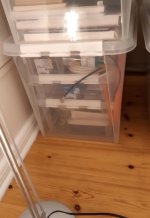
Phew - moving from 3 rooms / 80 sqm to a 1/35 was a real ordeal. But I'm very happy to have downsized - what a relief to sell and recycle 2/3 of ones "things". Love the new place. So I'm eager to continue with the recording system as soon as I have hade the pleasure to host a few gatherings and small parties. All good 🙂 and FGFR is neatly and safely stored in its plastic container.
//
//
Attachments
Coming to some sort of order here comes a steady stream of friends to visit which is nice but hinder me to open up the box as it will have to be placed on the dinner table and as that is placed in the only 1 room I now live in, its a bit problematic 😉 Anyways, the last thing happening after my mono street recording was that a very short bridge cable fell out of the board and I, at that time, could not figure out where it came from. Builds like this don't take movement very well and it made me want to do a PCB to mount most of the components on. So I have decided to do this before the making of the second one and thus, rebiuild the first one. It will be much better and now that I have the experience of assembling one I feel it will be easier to design such a board.
So either I try do use Eagle or some other EDA or rather, I would like to draw it "by hand" in my 2D CAD tool but I don't know how to transfer that into Gerber as I do want to use a PCB manufacturing house to just send a file and get boards back.
Any hints on if it is possible to do Gerbers without a proper E-CAD application?
Really eager to do the first stereo recording 🙂
//
Wow -- 35m² sounds awfully compact!
Any chance that it would be easier/faster to design on your familiar 2D CAD, then have a somewhat easier time manually transferring the design to other CAD software that can generate Gerbers?
I've never heard of someone producing a set of Gerbers manually. Of course, there are folks on here that know tons more than I do about it.😉
Cheers
Last edited:
Thanks - I hope I can get som hints on how to do that 🙂 Downsizing has been a great experience and I can recommend it - a fantastic relieve to have been able to get rid of a lot of stuff not used! Hopefully I will be able to expand later in an other location - say within a year or so 🙂
//
//
Com to think of it - maybe a can make a jpg etc of what I want on both sides, create a round board in an EDA program and just add a bottom and top silk layer and thats it - I have the traces - will probably have to drill myself but that would be OK I think 🙂
//
//
Maybe after all - TGIAutoRouter 🙂
EasyEDA.
//
EasyEDA.
//
Attachments
Last edited:
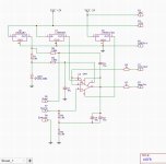
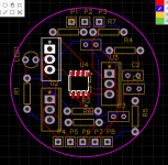
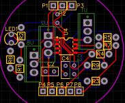
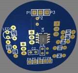
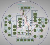
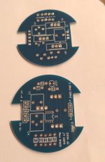
Now I think I might have something that I could order. If this works it will give a lot of more confidence in handling the board and the chance that 2 boards are similar in performance. Juts need to check a few distances on the built board and confirm that the PCB could work. Then I will order boards. If Marcel still reads this I would appreciate a quick glance on the schema to check that I didn't do any dodods in the transfer 🙂
Attachments

Last edited:
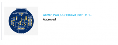
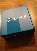
"Thanks for placing your order on JLCPCB.COM. Your order has been approved and put into production. You can review your order status at any time by logging into your JLCPCB Account and viewing your order history."
🙂
The picture attached to the above message shows the cutouts as lines - oh well, some sawing in worst case...
EasyEAD was OK for me. I have had prior experience in cad for PCB but it was a long time (20y) ago - still I'm sure that helped despite the long hiatus.
//
🙂
The picture attached to the above message shows the cutouts as lines - oh well, some sawing in worst case...
EasyEAD was OK for me. I have had prior experience in cad for PCB but it was a long time (20y) ago - still I'm sure that helped despite the long hiatus.
//
Attachments
Last edited:
11 USD for 5 boards ink shipping and "tax" (?) - there is probably an additional 25% surprise at the border 🙂
//
//
Attachments

Last edited:

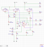
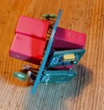
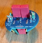
That was like a breeze compared. I made at least 2 dodos with the board design but both recoverable at stuffing time. To put one cap on each side in the same position (C3/C4) makes me wonder about my state... 🙂 But with a little "floating" mounting style on one of them I could reach to solder from the component side 🙂 - high density build! Some silicone here end there and it will be fine. Silicone is OK with electronics - right?
The other one is a silk error where I apparently seem to have mixed V+ and V- ... well well...

This felt much more safe and secure in terms of mounting. Good.
//
The other one is a silk error where I apparently seem to have mixed V+ and V- ... well well...
This felt much more safe and secure in terms of mounting. Good.
//
Attachments

Last edited:
- Home
- Source & Line
- Digital Line Level
- Fixed gain field recorder?