I think most want to be sensitive to the real world consequences of their actions. I do.
Mr. Pass said this
And he also said this in 2019 about a production amp. . .
Are cloners using that schematic? Are distributors upset/injured/bothered/tolerant by/of its existence?
I am biased of course and really want to see and try to understand lhquam's effort
A lhquam F8 schematic and real deal FW F8 schematic aren't the same unless one particular person says they are.
Also . . . Mr. EUVL, can I ask about the 20khz performance of the SS Jfets I got from your group buy? 😀
Mr. Pass said this
Points to consider:
On the downside -
PL and FW work through established distribution worldwide. Distributors
have been tolerant of DIY efforts to date, but have made it clear that
they don't like PL and FW stuff as kits or public schematics.
This is partly because of cloners and partly because it reduces the
appeal of commercial product as they see it.
Also, complete technical information gives the competition something to
badmouth, and/or copy...
And he also said this in 2019 about a production amp. . .
EUVL's schematics above look fine to me if you want to build a J2.
And if you want to DIY your own, be my guest.
Dual J109's gave me more front end bias and greater transconductance.
The R100 Jfets were selected for low leakage, but it's not a big issue.
There was a good build with IRFP240's on the mu follower, but we elected
to stay with the Jfets for all devices.

Are cloners using that schematic? Are distributors upset/injured/bothered/tolerant by/of its existence?
I am biased of course and really want to see and try to understand lhquam's effort
A lhquam F8 schematic and real deal FW F8 schematic aren't the same unless one particular person says they are.
Also . . . Mr. EUVL, can I ask about the 20khz performance of the SS Jfets I got from your group buy? 😀
I match the R100's as a matter of course while I am testing for high frequency
distortion, which is variable I am most interested in.
In a channel at 1W / 20 KHz into 8 ohms, they vary between 0.05% and >0.2%
Fortunately only a minority are in the high category.
The SS in the GB are matched at 100Hz, 55"C, in continuous mode.
If you want them matched at 20kHz, I think the easiest solution is to buy a First Watt amp.
Patrick
If you want them matched at 20kHz, I think the easiest solution is to buy a First Watt amp.
Patrick
I like this quote too. 🙂
On the upside -
I like doing DIY. It gives me a great outlet for creative efforts that don't
fit my commercial agenda.
I like DIYers - they are the happiest audiophiles I know, and are
remarkably nice and self-sufficient.
So what's not to like?
Why is on the FW site the J2 marked as SE and the F8 as descendent as PP?
As ZM sez, Typo.

Later: Fixed it.
Last edited:
Some comfort for ZM 🙂: My equations are not matching the simulations and neither achieve the THD levels without open-loop-gain about 12dB-20dB above what has been suggested for the F8. generg has similar results.
My equations are not matching the simulations and neither achieve the THD levels without open-loop-gain about 12dB-20dB above what has been suggested for the F8. generg has similar results
Should there be a source resistor on the semisouth Jfet? that would reduce the open loop gain.
to our amusement and puzzlement and unavoidable reason for  , Master is dealing with simulations only for Xover work
for amps , his Brain is perfectly attuned Simulator
, Master is dealing with simulations only for Xover workfor amps , his Brain is perfectly attuned Simulator
and I am only a "simulator" ......pretending too now something......
😎😎
for this I should get the "blue moons award"
😀
😎😎
for this I should get the "blue moons award"
😀
Couldn’t agree more. I reckon it’s cool for us to guess what Nelson was aiming for based on the clues that he generously lays out 🙂The motivation of Nelson to publish any schematics of his is, I am sure, not only to encourage people to build amplifiers.
It is also about educating people on analogue circuitry and how they work.
So if someone were to take a generalised / simplified schematics in the public domain, and publish a mathematical analysis of it, I cannot see how that contradicts Nelson's motivations.
A generalised analysis says nothing about the actual amplifier design, including component values and choices, matching details, power supplies, etc.
What I personally find much more offensive is for those people who have access to the original product details to clone and sell copies of them in private.
That, to me, is 100% theft.
Only my personal view,
Patrick
Lots of learning ensues as a consequence ... which makes it all worthwhile !
So pls don’t hold back :0
Should there be a source resistor on the semisouth Jfet? that would reduce the open loop gain.
This is done in the J2, in this way the OLG is around 50dB. But the nice new thing is that Nelson eliminates the source resistor for the Semisouth in the F8 and seems to compensate this with less gain in the F8 frontend.
I estimate in Spice that the source resistor at the Semisouth in J2 reduces the OLG about 6dB.
Ok generg, I removed the source resistor and biased the front end to lower the gain. The open loop gain is 5db less than what you said was the j2. Distortion is .02. I could still try and lower the front end gain more and change the optocoupler bias resisters to improve distortion.
...
Thinking R11 should maybe be smaller, maybe around 1k.
...
I think understanding and solving this is the critical problem.
I think I get why 2.6k at R11 sounds clearly better. Please correct me if I'm off here. R8 and R11+jfet create the divider for feedback. When the jfet is most resistive, more signal is sent to ground. When its least resistive, more feedback is applied and you have distortion because of variations in gain. The higher the signal voltage, the higher the ratio which explains steadily climbing distortion as you go up in power. Setting R11 to 2.6 minimizes the percentage of resistance the jfet contributes. Going higher, the jfet starts running out of juice.
My thinking was I can send a portion of the discarded feedback signal somewhere as feedback ??? which also varies with the amplituted? (way out of my element as to what to call it. Maybe resistive modulation?). Simple change. I think this schematic fixes that specific issue. For the first time I am able to split the output resistors to the ratio like the ones on the ACP+. If you're liberal with your definition of V with a circle around it, it matches the simplified schematic too.
The shape and value of the simulated distortion at 1k matches the F8 manual well. R3 has a great deal of impact on the phase of distortion. 7.5k is a much better value there than 3k5 I think.
Attachments
Re F8
Have you built it yet?
How does it compare with the other amps you've built?
Thanks,
Scott
Built a circuit in Ltspice using your schematic and after changing a few values come up with Nelson's distortion and CLG values and frequency reponse almost exactly.You mention no R6,I left the circuit as you have it plus I added a gate stopper on the lower mosfet.Why do you say no R6?
Have you built it yet?
How does it compare with the other amps you've built?
Thanks,
Scott
hello everyone I am passionate about reading all the discussions here of the posts but in the end I conclude that .... if in some way this project leaves similar satisfactions to the J2 and F8 why not publish some photos of the realization or of the working scheme?
I have the topic and was brought to another discussion post.
I was preparing to build the EUVL J2 Clone and I stopped as intrigued by these schemes also because we do not use the output Jfet which are too expensive
I await news thanks to all
I have the topic and was brought to another discussion post.
I was preparing to build the EUVL J2 Clone and I stopped as intrigued by these schemes also because we do not use the output Jfet which are too expensive
I await news thanks to all
Just want to share my own version that also designed base on the concept schematic posted on this thread.
IF8 MOS - PicZ.in.th
Welcome for comments.
IF8 MOS - PicZ.in.th
Welcome for comments.
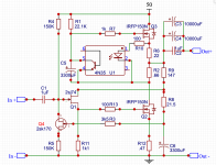
August last year, I posted a spice file of a DC coupled "F8".
First Watt website update
First Watt F8
As said before, it is purely my speculation and bears no relations to the original.
I don't have a F8. I have not seen one. I have no idea of the original component values.
But a brave guy went ahead to build one according to the above schematics.
To quote him :
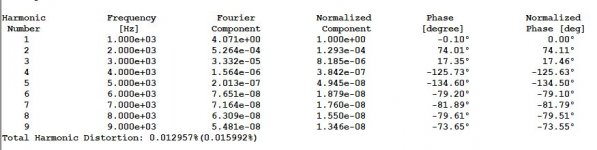
"I have built up Patrick's board and no surprises but it is quite close to the sim.
I just used standard values and let it come up to temperature.
Bias started at 1.40A and didn't change much as temperatures stabilized.
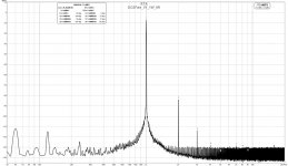
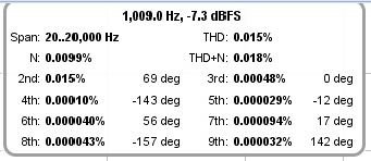
THD matches the sim even down to the phase angle (relatively close).
I used 0.68/0.68 and 1.0/1.5 values for the 3W positions.
THD is 0.015% and is pretty much all H2 (negative phase).
H3 is almost 30dB down from H2.
Heatsink temperature stable at 47C (about the same size as diyA store 4U/300mm).
DC offset started at 15mV and stable at 20mV after fully warmed up."
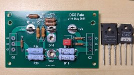
And we called in DCSFate.
Cheers,
Patrick
.
First Watt website update
First Watt F8
As said before, it is purely my speculation and bears no relations to the original.
I don't have a F8. I have not seen one. I have no idea of the original component values.
But a brave guy went ahead to build one according to the above schematics.
To quote him :
"I have built up Patrick's board and no surprises but it is quite close to the sim.
I just used standard values and let it come up to temperature.
Bias started at 1.40A and didn't change much as temperatures stabilized.
THD matches the sim even down to the phase angle (relatively close).
I used 0.68/0.68 and 1.0/1.5 values for the 3W positions.
THD is 0.015% and is pretty much all H2 (negative phase).
H3 is almost 30dB down from H2.
Heatsink temperature stable at 47C (about the same size as diyA store 4U/300mm).
DC offset started at 15mV and stable at 20mV after fully warmed up."
And we called in DCSFate.
Cheers,
Patrick
.
Attachments
- Home
- Amplifiers
- Pass Labs
- First Watt F8