Since we are strolling down off-topic memory lane,
Here is a photo, and also a couple of photos of four Stasis 1's being restored
in my shop. You can see the output stages and the stripped down power
supply part of the chassis.
😎
I remember hearing and SEEING the Stasis 1s at "Oslo Hifi Center" circa 1980. I do not remember the front end at all, some turntable maybe with an EMT, maybe the SL-10 preamp, however pretty sure the Infinity RS-4.5 was the speakers. But I came there to see and hear the new Stasis 1s and was awestruck. This was something to adore for a young man who still had not seen "Gone with the Wind"....
Pretty sure the Infinity RS-4.5 was the speakers
Those are the speakers used by the present owner.
Don't anybody get any ideas, this work is for an old friend...
😎
Those are the speakers used by the present owner.
Don't anybody get any ideas, this work is for an old friend...
😎
I thought we were all friends here.
Hahahaha
😛
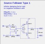
After considerable equation crunching I came up with what appears to be an elegant solution for a source-follower output stage having only positive feedback and requiring no extra sense resistor like the one in post #646. The inherent internal resistance Rint of the source follower stage provides the sense resistance, and the Type-1 feedback topology equations of the common-source amplifier have been modified for the source follower. What appears to be negative feedback to the input stage is really just generating the voltage difference across Rint.
What is important about this circuit is that it can be used for a balanced (bridged) amplifier, whereas the circuit of post #646 cannot.
What is important about this circuit is that it can be used for a balanced (bridged) amplifier, whereas the circuit of post #646 cannot.
Attachments

It appears to me that post #684 http://www.diyaudio.com/forums/pass-labs/275921-first-watt-f7-review-69.html#post4736734 is nothing more than a variant of Hawksford Error Correction (HEC).
It appears to me that post #684 http://www.diyaudio.com/forums/pass-labs/275921-first-watt-f7-review-69.html#post4736734 is nothing more than a variant of Hawksford Error Correction (HEC).
Hello lhquam.
Will HEC grant its amp an infinite damping factor?
Please clarify your definition of Rin. Suppose a preamplifier has a zero ohm output impedance. It drives the input of the amp [in above posts] through a 3.3 K series resistor. It is clear that Rin =3.3K. Suppose the input of the power amp has a 47 K resistor return to ground. Would you then say that Rin is actually 3.3K//47K?
The input impedance of the above power amp is quoted as ~50 K. What's one to use for Rin in your equations above:. 3.3 K, 3.3K//47K or 47K?.
Antoinel: My recent posts have paid no attention to Rin, the amplifier input impedance, but here is how to define it. Another resistor R2 is needed in order have a defined and positive input impedance. Without R2, the input resistance defined by R1eff in the schematic below is negative. In order to get in input impedance of Rint, add R2=Rint||(-R1eff).
Attachments
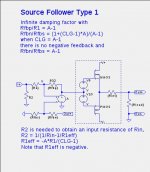
Antoinel: My recent posts have paid no attention to Rin, the amplifier input impedance, but here is how to define it. Another resistor R2 is needed in order have a defined and positive input impedance. Without R2, the input resistance defined by R1eff in the schematic below is negative. In order to get in input impedance of Rint, add R2=Rint||(-R1eff).
Thanks lhquam.
Here are the equations for a differential gain stage and source-follower output stage which allows one to choose the output impedance and overall closed-loop gain (CLG), thus also choosing the amount of negative feedback.
Attachments

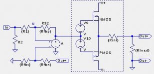
Here are the equations for a differential gain stage and source-follower output stage which allows one to choose the output impedance and overall closed-loop gain (CLG), thus also choosing the amount of negative feedback.
Hello lhquam.
The models in your two recent posts suggest that positive voltage [instead of current] feedback was used. In my experiments with positive voltage feedback [PVF], CLG increased, output noise increased, and the extent of PVF must be a fraction of the extent of negative feedback; e.g. 90% max to prevent oscillation.
The models contain both voltage and current feedback.
In the Type-1 topology, voltage at the top of Rsen is the sum of the voltage across Rload plus the voltage across Rsen, which is a measure of output current.
In the Type-2 topology, the voltage at the top of Rload is the sum of the voltage across Rload plus the voltage across Rsen, which is a measure of output current.
F7 uses a negative feedback loop wrapped in a HEC error correction loop
It has become clear to me that the feedback structure of the FirstWatt F7 is equivalent to a negative feedback loop surrounded by a "degraded" Hawksford Error Correction (HEC) loop. By degraded I mean the the resulting output impedance is Rint rather than zero.
Searching this thread, this is the first observation about the relation between HEC and the combination of positive and negative feedback.
It has become clear to me that the feedback structure of the FirstWatt F7 is equivalent to a negative feedback loop surrounded by a "degraded" Hawksford Error Correction (HEC) loop. By degraded I mean the the resulting output impedance is greater than zero.
Searching this thread, this is the first observation about the relation between HEC and the combination of positive and negative feedback.
Retraction: F7 doen't implement HEC
I must retract my previous post. The F7 senses the output current thru a sense resistor, which allows it to reduce the output impedance using positive feedback.
That is different from HEC which senses the error voltage between the input and the output of the unity gain output stage.
The circuits I show in posts 684, 685, 688, and 690 of an amplifier with a source follower output stage do implement HEC.
Hello lhquam. The attached schematic maybe described as a Current Source Amp [CSA] which uses Positive Current Feedback [PCF]. Here are its salient details:
1. The power output stage [diyF4] is used as common source amplifier with a voltage gain of ~ 8; instead of a power buffer.
2. Note the location of Vout in the schematic.
3. The AC current at the joined drains of the Mosfets which flows through the 8 Ohm loudspeaker load is exactly equal to the AC current which flows through the 1.1 Ohm load resistors at the joined sources of the Mosfets.
4. It follows that the voltage drop across the 0.1 Ohm sense resistor is proportional to the current flowing through the loudspeaker.
5. Alternatively, the full voltage drop across the 1.1 Ohm resistors is also proportional to the current flowing through the loudspeaker.
6. The resultant sense voltage [PCF] is forwarded to the non-inverting input of the preamplifier via Rpf. This preamp is shown as a voltage source amp which may [as shown] or not use overall negative feedback.
Attachments

Wrapping Positive Current Feedback around an existing Amplifier
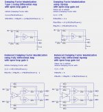
After considerable algebraic circuit analysis I present four circuit topologies for wrapping positive current feedback around an existing amplifier. The first two topologies are for unbalanced voltage amplifiers with voltage gain B and output resistance Rint, and the other two topologies are for balanced (bridged) voltage amplifiers, each with voltage gain B and output resistance Rint. The positive current feedback is implemented using the current sense resistor Rint in the Type-1 position relative to the speaker load of post #442 http://www.diyaudio.com/forums/pass-labs/275921-first-watt-f7-review-45.html#post4585617. For each amplifier type, there is a circuit using a differential amplifier with voltage gain A, and another circuit using an opamp with high open-loop gain Aol. To simplify the results shown here, Aol is assumed to be infinite for the opamp circuits, and the damping factor of each resulting amplifier using positive current feedback has been made infinite, ie. the internal output resistance is zero. It should be straight-forward to implement any of these topologies as a box a small power supply and RCA (or XLR) connectors and binding posts to connect to the existing amplifier. In each circuit diagram shown below, a dashed box surround the existing amplifier(s).
After considerable algebraic circuit analysis I present four circuit topologies for wrapping positive current feedback around an existing amplifier. The first two topologies are for unbalanced voltage amplifiers with voltage gain B and output resistance Rint, and the other two topologies are for balanced (bridged) voltage amplifiers, each with voltage gain B and output resistance Rint. The positive current feedback is implemented using the current sense resistor Rint in the Type-1 position relative to the speaker load of post #442 http://www.diyaudio.com/forums/pass-labs/275921-first-watt-f7-review-45.html#post4585617. For each amplifier type, there is a circuit using a differential amplifier with voltage gain A, and another circuit using an opamp with high open-loop gain Aol. To simplify the results shown here, Aol is assumed to be infinite for the opamp circuits, and the damping factor of each resulting amplifier using positive current feedback has been made infinite, ie. the internal output resistance is zero. It should be straight-forward to implement any of these topologies as a box a small power supply and RCA (or XLR) connectors and binding posts to connect to the existing amplifier. In each circuit diagram shown below, a dashed box surround the existing amplifier(s).
Attachments
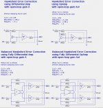
Wrapping Hawksford Error Correction around an existing Amplifier
Here are circuits for wrapping Hawksford Error Correction around existing amplifiers. The primary difference from the previous posts is the the current sense resistor(s) Rint have been eliminated and the voltage difference between the input and output of the existing amplifier is fed back to a differential amplifier.
Here are circuits for wrapping Hawksford Error Correction around existing amplifiers. The primary difference from the previous posts is the the current sense resistor(s) Rint have been eliminated and the voltage difference between the input and output of the existing amplifier is fed back to a differential amplifier.
Attachments
A major difference between positive current feedback (PCF) and Hawksford Error Correction (HEC) is that PCF shouldn't change the harmonic structure of the amplifier, whereas HEC attempts to remove all differences between the output and the input (multiplied by the closed loop gain), including the harmonics. I need to run some simulations to verify this conjecture. If anyone is really interested, I can provide the systems of circuit equations used to produce all of the resistor ratios shown in the circuit diagrams.
- Home
- Amplifiers
- Pass Labs
- First Watt F7 review