sndlvr, yes, those are important resistors. Blank on the Channel A board is for R2; blank on Channel B board is for R1. Earlier post noted error when boards were stenciled.Thank you most honorable 6L6, I am midway in my build of the F6 and have been working around the absence of the jpgs but am now at a point where I could really use them. Also while I have you, there are two places on the F6 PCBs that look like they are for resistors but are not marked (see attached photo). I'm sure this has been asked before, but what are they for? Many thanks.
Hooray, They are back! Thanks!!Ooh… this has a lot of broken photo links in the first post. Ouch. I‘ll go looking for them.
Zen Mod, I pulled the MOSFETs, which seem to test as OK. No continuity between D and S. On an inexpensive transistor tester from Amazon, which identifies them as "N-E-MOS", and applies 4.17V, all the tested values are similar to a new MOSFET, though I don't truly understand whether they're meaningful since the symbols used don't match those in the IRFP240 spec: Vt=3.6V, Cg=2.49nF, Rds=0.4 ohms, and there's 579mV showing next to the diode symbol that connects S to D.if you're going to replace mosfet(s), it's best to pull them both from circuit, and then test everything else under voltage, prior to installing replacement mosfets ............ and you'll install new ones only when you're sure that everything is OK
zeners need to show adequate voltage across
trimpots need to bring full span of min to max voltage to mosfet gate resistors; upper one ref. to GND, lower one ref. to neg rail
voltages across JFet source resistors need to be so-so equal
mosfet source resistors checked with ohmmeter - it's low value but if you're in doubt - replace them ....... even if possibility of them gone Dodo (and to short, instead to usual ope circ) is extremely small
of course, mosfet isolation from sinks and proper thermal interface - goes without saying
I pulled one 6V8 zener, Z1, which tested fine out of the circuit. Lifted one lead on Z2 and it also tested fine. Replaced Z1 and resoldered the Z2 lead. Getting 6.85V across Z1, 6.67V across Z2 in live circuit with no MOSFETs.
P1 and P2 test fine 0-5K when the circuit is unpowered, but when they are turned full range in the powered circuit they make no change in the voltages measured across the MOSFET source resistors R1 or R2 when those source resistors are referenced either to ground or V- (PSU is making a stable 24.04V at V+ and V-).
Voltages across signal transformer pins 1-3 and 2-4 are identical at 0.655V when the circuit is powered, which yields 0.0512A if I'm doing the math right. Voltage across 18 ohm JFET source resistor (R4) stabilizes at 0.8V. These values are way higher than equivalent values in the good Channel B circuit: 0.012V across the 1-3 & 2-4 pins, 0.0V across R4. But that channel has MOSFETs in the circuit.
The MOSFETs and all other components testing okay seems to leave the JFETs as the culprits. Are the channel-to-channel comparative voltage differences across the transformer pins and R4 values, and the trimpots failing to change voltage across the MOSFET source resistors, indications that one or both JFETs are bad? I can pull them and stick them in the transistor tester, but chances are good I won't know what the values it shows mean.
OK, will do, thanks. Is there anything else I should check before I put in new JFETs and MOSFETs?50mA is way too high for JFets
pull them out and check with simple JFet matching jig
9V will do as PSU
besides continuity of xformer windings and generally checking all resistors, not much else
you already checked upper and lower biasing circs, so that's pretty much all
take care of mosfet-sink isolation
you already checked upper and lower biasing circs, so that's pretty much all
take care of mosfet-sink isolation
First time I've pulled MOSFETs. I know the circuit got hot because of runaway bias, is this bubbling unusual?besides continuity of xformer windings and generally checking all resistors, not much else
you already checked upper and lower biasing circs, so that's pretty much all
take care of mosfet-sink isolation
Attachments

Nodough, this might be a good opportunity to add IRFP150 mosfets to your list. They don't have to be matched but if you get them from the a place like mouser, they should be fairly well matched anyways. TungstenAudio has mentioned FQH44N10 being a really good option. I have done the IRFP150's without any other mods so I know I can recommend them.
Best of luck! I hope you get things sorted.
https://www.mouser.com/ProductDetail/844-IRFP150PBF
Best of luck! I hope you get things sorted.
https://www.mouser.com/ProductDetail/844-IRFP150PBF
Zen Mod, you have saved me. (Well, my F6 build, anyway. Pretty sure I'm beyond redemption.) Replaced the MOSFETs, source resistors, a zener and the JFETs. Might be premature to declare success, but it was easy to bias and, after 20 minutes, is holding bias, aside from the normal warming up slow creep. Back to where I started before the arc, it's again playing music with no hum whatsoever, so far... I have learned my probe/power off lesson for sure. Can't thank you enough for all your patient assistance and tolerance of my ignorance.
6L6, wow, this can be done by novices, but not without your invaluable guides (I did the ACA (two) and B1 as well). Thank you [Loud clapping].
Of course, adding my undying gratitude to Mr. Pass for his ridiculous smarts and generosity.
Mikerodrig27, thanks for the MOSFET suggestion. Didn't see it till now, but I had already bought 10 IRFP240s from Mouser and wouldn't have wanted to wait several more days to see if the fixes would take. And you're right, presumably from the same lot they all tested within a couple % of each other. if I get the gumption to fiddle around someday, maybe I'll give the IRFP150s a go.
Sounds good. I did the popular Pico Dumb Mod and swapped in IRFP150's at the same time. The pico mod is three LED resistors in series to replace the zener diode. There is a thread on it. The LED mod helps the amp to get to temperature faster from cold. The IRFP150's ad a little more detail to the sound. The F6 is a wonderful amp as is with the IRFP240's. Enjoy it! I have thoroughly enjoyed mine for a couple of years now.
I came across the suggestion to replace the zener with LEDs a couple of times - after I had already placed the zeners, of course. Is the idea to replace both zeners with LEDs or only the bias zener, Z2? Getting some low-level hum on the left channel now (channel A board, same one I allegedly fixed). Right channel remains quiet, so likely not a PSU issue, I'm thinking.
The pico dumb mod won't solve your hum issue. It is just something you can try after amp is in working order if you like. It is three resistors tied in series in place of the bias and offset zeners. Works good.
Do you have a picture of your amp? Maybe a few?
Do you have a picture of your amp? Maybe a few?
Yes sir. Channel A is the hummer. Spectrum app has it between 99-125 Hz, so I'm guessing it's 120Hz. Both channels have it, but can only hear it on the right channel (B) when my ear is right up against the woofer, which is acceptable. I can hear the channel A hum from my listening seat, barely, when no music is playing.
When I look at the two amp boards, the only noticeable difference in assembly is the height of the JFETs. When I replaced the JFETs in channel A, I left the leads at full length, so the JFETs sit up higher, which puts their tops roughly level with the midpoint of the Jensen signal transformer. What's the chance that tranny is introducing hum through those JFETs? Worth the effort to lower them? Is there a best practice height that should be considered with those types of transistors?
When I look at the two amp boards, the only noticeable difference in assembly is the height of the JFETs. When I replaced the JFETs in channel A, I left the leads at full length, so the JFETs sit up higher, which puts their tops roughly level with the midpoint of the Jensen signal transformer. What's the chance that tranny is introducing hum through those JFETs? Worth the effort to lower them? Is there a best practice height that should be considered with those types of transistors?
Attachments
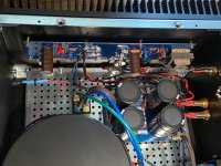
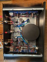
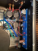
I used rubber spacers to raise the perforated base plate that the PSU is mounted to about 3/4" above the bottom cover. AC wiring runs under the base plate. That tip came from an early post by Zen Mod, though I believe he used rigid plastic spacers. Because the rubber spacers electrically isolate the heatsink sinks from the star-grounded base plate, I used grounding straps to tie the sinks to the base plate.
Last edited:
OK, great! That will simply things. Thx!👍you have too many GND bridges between cap pcbs
you need to have just one 🙂
- Home
- Amplifiers
- Pass Labs
- F6 Illustrated Build Guide