Is there a problem with .jpg images not showing or able to open? Thanks This is in the F6 Illustrated Build Guide
"This link" https://www.diyaudio.com/community/threads/f6-illustrated-build-guide.277850/
Is working fine for me. (Firefox)
Is working fine for me. (Firefox)
Ok. Will check my computer for problems. Using Chrome. Will try Firefox and or check settings on my browsers. Forgot to say thanks
I’m almost always on my iPhone when checking in. Maybe this is a Safari issue? Most of the jpg images are not showing. This thread is from 11/15/2013 by 6l6
Switched browsers and .jpg pictures come up. Oops sorry, they did not. Must be some settings on my end.
Hey,
I don’t mean to send you down the rabbit hole. But I’ve noticed similar broken photo links on several threads. I don’t think this is associated solely with the new software/website. I did check my browser settings but nothing looked out of place. No worries either way.
Regards
I don’t mean to send you down the rabbit hole. But I’ve noticed similar broken photo links on several threads. I don’t think this is associated solely with the new software/website. I did check my browser settings but nothing looked out of place. No worries either way.
Regards
I believe Jim used picbucket, at first ...... which is Bad Juju
he became smarter later
though, Bad Juju is always getting back, price to be paid
he became smarter later
though, Bad Juju is always getting back, price to be paid
Hi all. Hoping someone can help me troubleshoot my F6 build. Completed the build in the Deluxe 4U chassis. Everything tested well, biased both boards to a stable 0.50V across R2 and DC offset was likewise stable at less than 5mV. Connected inexpensive speakers to check audio, and it sounded good. No hum in either channel, dead silent. Checked bias and offset one last time before installing chassis cover. As I removed my Fluke DMM retractable hook test probes from R2, I heard a pop from the speakers, and then hum started to slowly build in volume in the left speaker, which is Channel A. Situation is very similar to what HeyBill described in post #3458.
I read all responses to HeyBill's troubleshooting and tried what was suggested. All component values are correct. Boards have 6V8 at Z1 & Z2; 3.3K R7 & R8; 110R R11 & R12. Components test good in circuit as referenced to functional Channel B. PSU V+ & V- stable at 23.5V (and no issues with Channel B). I don't have an oscilloscope.
LED lights on Channel A. Diodes, MOSFETs and JFETs pass diode test (I think) in circuit. Signal transformer (Jensen) tests proper for continuity and resistance. Big clue that I can't decipher is that I'm getting runaway bias voltage across both R1 and R2, and Q1 and Q2 likewise go into thermal runaway. I haven't left the amp on for more than a few moments since this happened, but was able to measure voltage across Q1 source and drain, which seems to top out around 4.25V, but as mentioned, the bias voltage across R1 and R2 keeps rising rapidly, so I don't leave the amp on for more than a minute or so - shutting it off before it bias gets to 1V. Measured the temp at pin 2 on Q1 as 75C the last time I had the amp on. I have not changed settings on P1 and P2 since this happened. I suppose I could dial P2 all the way to 0R to see if bias still runs rampant.
I plan to replace Q1 & Q2 (if for no other reason than one of them, Q2, got hot enough to produce a thin curl of smoke at pin 2). Before I energize Channel A again, is there anything else I should consider replacing so I don't potentially damage the new MOSFETs? What could be the cause of the loss of bias control? Could the JFETs have been damaged and is there a way to test them for damage in circuit?
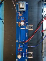
Should add that this hum is not the typical, low level ground loop hum. It's loud, like something is broken in the circuit, and it starts (softly) when the bias gets to about 0.3V across R2 and build to loud quickly as the bias climbs. Photo attached (note, removed screws and washers from Q1 & Q2 just before taking photo).
I read all responses to HeyBill's troubleshooting and tried what was suggested. All component values are correct. Boards have 6V8 at Z1 & Z2; 3.3K R7 & R8; 110R R11 & R12. Components test good in circuit as referenced to functional Channel B. PSU V+ & V- stable at 23.5V (and no issues with Channel B). I don't have an oscilloscope.
LED lights on Channel A. Diodes, MOSFETs and JFETs pass diode test (I think) in circuit. Signal transformer (Jensen) tests proper for continuity and resistance. Big clue that I can't decipher is that I'm getting runaway bias voltage across both R1 and R2, and Q1 and Q2 likewise go into thermal runaway. I haven't left the amp on for more than a few moments since this happened, but was able to measure voltage across Q1 source and drain, which seems to top out around 4.25V, but as mentioned, the bias voltage across R1 and R2 keeps rising rapidly, so I don't leave the amp on for more than a minute or so - shutting it off before it bias gets to 1V. Measured the temp at pin 2 on Q1 as 75C the last time I had the amp on. I have not changed settings on P1 and P2 since this happened. I suppose I could dial P2 all the way to 0R to see if bias still runs rampant.
I plan to replace Q1 & Q2 (if for no other reason than one of them, Q2, got hot enough to produce a thin curl of smoke at pin 2). Before I energize Channel A again, is there anything else I should consider replacing so I don't potentially damage the new MOSFETs? What could be the cause of the loss of bias control? Could the JFETs have been damaged and is there a way to test them for damage in circuit?
Should add that this hum is not the typical, low level ground loop hum. It's loud, like something is broken in the circuit, and it starts (softly) when the bias gets to about 0.3V across R2 and build to loud quickly as the bias climbs. Photo attached (note, removed screws and washers from Q1 & Q2 just before taking photo).
Attachments
Last edited:
if you're going to replace mosfet(s), it's best to pull them both from circuit, and then test everything else under voltage, prior to installing replacement mosfets ............ and you'll install new ones only when you're sure that everything is OK
zeners need to show adequate voltage across
trimpots need to bring full span of min to max voltage to mosfet gate resistors; upper one ref. to GND, lower one ref. to neg rail
voltages across JFet source resistors need to be so-so equal
mosfet source resistors checked with ohmmeter - it's low value but if you're in doubt - replace them ....... even if possibility of them gone Dodo (and to short, instead to usual ope circ) is extremely small
of course, mosfet isolation from sinks and proper thermal interface - goes without saying
Thanks, Zen Mod. Want to be sure I understand your guidance
I will replace both Q1 and Q2, but only after the energized circuit tests OK with them out. I believe I read that they do not need to be matched, but I bought 10 so I'll pick two that are closest in value.
Zeners should have adequate voltage across their leads when energized, and that should be something above 6.8V?
To test the trimpots full range, do I measure as I would to set bias (for P2, voltage across R2) and DC offset (for P1, voltage across output + and ground)?
I'm not sure which resistors are the JFET source resistors. Are they R4 (18R) & R8 (10K)? Will this test confirm the JFETs are operating properly?
MOSFET source resistors check good now (0.8R for R1 0.56R and 0.7R for R2 0.47R), but I'll likely replace them just because.
Keratherm pads look fine - no punctures or burnt marks, but I'll replace them as well.
This presumed arcing (the pop I heard) has made me gun shy about attaching probes to R2. Pretty sure I did not short the probe to another component. Aside from jamming the probe's hook between Q1's pins, it's physically impossible for the probe to short anything there. The metal part of the probe is too short to connect any two components in the area of R2/Q1. Also, when I replaced the retractable hook probes with sharp, pointy probes and touched R2 (carefully), that pop occurred again. Not every time, but a couple of times. This seems to be arcing, though I see no spark. Thought it could also indicate a bad lead/solder joint on R2 or C2 (which can provide a tight squeeze for the probe), so I reflowed the solder. No improvement (hum still there). Is arcing unusual?
arcing is always unusual
now - because origin schematic is missing from post #1, it would be nice that you post your reference schematic, so we know that we are on same page, regarding parts nomenclature
input buffer is having one N and one P channel JFet, each having 10R resistor in source; voltage across each will say current through its JFet, thus will show functionality of same
zener voltage - probes on two ends of zener
trimpot voltage span - from full CW to full CW, measured ......... lets say - black probe at Anode of adjacent zener, red probe at adjacent gate mosfet resistor ....... so that way checking also adjacent signal xformer secondary
now - important rule when you don't have enough mileage - connect and disconnect tricky probes ( and clips are tricky!) only when circuit is powered Off
believe me - even after 158yrs doing these things - when small clips are in tight/critical place, I'm doing exactly the same - power Off, wait caps to bleed down, then fiddle with clips
Ah! That is an important probe tip, so to speak. Thanks! I will practice probe discipline from now on.

Are R7 and R8 the JFET source resistors? No, strike that. I changed those to 3.3K based upon your advice.
OK, thank you, 6L6. So, for ZM's advice on checking functionality of JFETs, I just need to check that voltage across R4 remains stable? As well as the ability to properly set bias and DC offset...The source resistance in the Jfet front-end is R4 and the DCR of the transformer windings.
Last edited:
ha, confusion - I was looking at schematic from Papa's article in my PC
final iteration is obviously lacking 10R in sources of JFets
as Jim sez - voltage between pins 1 & 3 (xformer) should show upper JFet current
same - pins 2 & 4 , for lower JFet current
now, that will show similarity of these two currents
if you want to compute them - that goes as I=U/R, where U is measured voltage between pins and R is measured ohms between pins, when amp is Off
I am using Firefox on a Mac and many of the image links on the file you linked to are not showing."This link" https://www.diyaudio.com/community/threads/f6-illustrated-build-guide.277850/
Is working fine for me. (Firefox)
Thank you most honorable 6L6, I am midway in my build of the F6 and have been working around the absence of the jpgs but am now at a point where I could really use them. Also while I have you, there are two places on the F6 PCBs that look like they are for resistors but are not marked (see attached photo). I'm sure this has been asked before, but what are they for? Many thanks.Ooh… this has a lot of broken photo links in the first post. Ouch. I‘ll go looking for them.
Attachments

Danced around a bit, but R eventually settled in (in cicuit) as 12.8 ohms for 1 & 3 and for 2 & 4. Will check voltages when I fire it up again after removing the MOSFETs.ha, confusion - I was looking at schematic from Papa's article in my PC
final iteration is obviously lacking 10R in sources of JFets
as Jim sez - voltage between pins 1 & 3 (xformer) should show upper JFet current
same - pins 2 & 4 , for lower JFet current
now, that will show similarity of these two currents
if you want to compute them - that goes as I=U/R, where U is measured voltage between pins and R is measured ohms between pins, when amp is Off
- Home
- Amplifiers
- Pass Labs
- F6 Illustrated Build Guide