Most likely yes.
I was able to bias the hockey pucks without any fancy techniques but it took over an hour for it to stabilise. I felt that wasn't really practical when you want to just turn on the amp and listen so decided to add the thermistor but it certainly wasn't necessary.
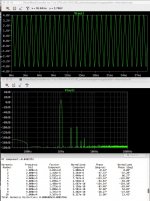
How much global feedback (GFB) are you throwing at your amp? I now have good simulations without degeneration, but a lot (> 16dB) of GFB is needed to get distortion levels comparable to XA25 Manual plots, unless you are willing to accept fairly high THD levels at high frequencies. Note the the XA25 Manual does not show a plot of THD vs. Frequency.
Around 15 to 16dB global feedback
There is a lot more local cascode feedback.
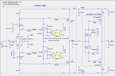
The front end is the key.
Have you tested high frequencey distortion with Toshibas based at 50mA, 100mA and 200mA?
I don't get too excited/concerned about distortion with the fundamental above 10kHz
When I finish up on the cases and test the first prototype I'll start getting more involved here.
There is a lot more local cascode feedback.
The front end is the key.
Have you tested high frequencey distortion with Toshibas based at 50mA, 100mA and 200mA?
I don't get too excited/concerned about distortion with the fundamental above 10kHz
When I finish up on the cases and test the first prototype I'll start getting more involved here.
Last edited:
I have recently learned some things about negative feedback amplifier stability what I was totally ignorant about. I found some very interesting information in these application notes. The important info is about the unity-gain stability criteria, which can extracted from the Bode plot. If the slope of the open-loop gain at the Closed-Loop Frequency Fcl is not greater than 6db/octave, then the amplifier is stable. The phase margin can be horrible, but if this criterion is met the amplifier will not oscillate, but it might overshoot.
- Analog Devices: Look particularly at page 20 (Ch 1.16). http://www.analog.com/media/en/training-seminars/design-handbooks/Basic-Linear-Design/Chapter1.pdf
- Intersil: Around page 8. http://www.intersil.com/content/dam/Intersil/documents/an94/an9415.pdf

OK I'm joining in the fun the pair arrived today!
Will be testing this weekend keep you posted will use 2Picodumbs circuit.🙂
Will be testing this weekend keep you posted will use 2Picodumbs circuit.🙂
Hi friends,
PR was so friendly to combine the best of both worlds.
His driver bias opto control idea with the thermistor stabilization of the IXYS.
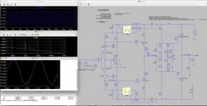
Spice data will follow....
I think it will be important that R18 and R20 is set so Idss of jfet produces voltage around/near vgs threshold of the mosfets for this to operate correctly. That is not too high.
R18 and R20 are set to give around 50mA.
With this circuit I could not see that 100mA for the drivers give less distortion.
With this circuit I could not see that 100mA for the drivers give less distortion.
Just to avoid any confusion for the front end circuit R8/R14 and R9/R16 are trimpots. 500 Ohms would be a suitable value.OK I'm joining in the fun the pair arrived today!
Will be testing this weekend keep you posted will use 2Picodumbs circuit.🙂View attachment 600747
Depending on the filtering up stream you may also want to leave space for a cap across R3 and R20.
I will reveal more details after I have built and tested, but the goal is always caveman-simple.
Thanks for the heads up but like you I'm keeping it "caveman simple" my front end is different again.
Will post picks and scope shots of my findings.
Have to careful here these things cost nearly $50 a piece here in Canada so will be taking extra care with the power supply!
Will post picks and scope shots of my findings.
Have to careful here these things cost nearly $50 a piece here in Canada so will be taking extra care with the power supply!
Here is alternate DUAL opto-bias circuit which should have both FE bias stability and FE output offset stability since the opto-bias circuit is referenced to ground rather than floating. It also has the advantage of not introducing resistors to the FE (Toshiba) MOSFET drains. With the bias circuits adjusted for minimal current injection at nominal operating temperature, the bias circuit should have virtually no effect on the gain and distortion of the amplifier. That is also true for the single opto bias circuit.
Attachments
in the footsteps of Nelson, Peter R., Lynn Q in optocoupler use.......😀
the question pr rose was ... how good are these dual and quad optocouplers really matched not to get too much offset with temperature.
Can anyone see that in the data sheets....?
the question pr rose was ... how good are these dual and quad optocouplers really matched not to get too much offset with temperature.
Can anyone see that in the data sheets....?
Attachments
Lynn checked my idea and sees some flaws concerning behavior with rising temperature.
So the race goes on..... :--))
So the race goes on..... :--))
Lynn checked my idea and sees some flaws concerning behavior with rising temperature.
So the race goes on..... :--))
The problem was not rising temperature in particular, but the lack of sufficient gain from just the photo-transistor internal to the opto and lack of sufficient low-pass filtering. The challenge is to introduce another non-inverting gain stage that has low impedance output. I have tried several circuits involving a common-drain (emitter follower) but the lack of voltage gain limited their performance.
Lynn checked my idea and sees some flaws concerning behavior with rising temperature.
So the race goes on..... :--))
I already told you about this.
Dumb bastards.
I'm not helping you blokes anymore. No respect. Hahaha
Almost finished drilling a million bloody holes.
Was gonna take a photo but it's not that exciting.
Was gonna take a photo but it's not that exciting.
- Home
- Amplifiers
- Pass Labs
- F4 Beast Builders