Are you implying that discrete regulators are better based on what you hear? If it is based on purely subjective opinions then no sweeping statements should be made. You should at least add something like "in my experience" to your statement.
What makes you believe you are in position to tell me what wording to use?
Please read my post again, I made pretty clear that expressed opinions are not the final truth.
If you have real measurements to back your statements why do you post irrelevant simulations as in post #6622?
Wouldn’t you mind to formulate this as “irrelevant simulations according my experience “ please?
Not really. You posted this: "low enough and flat in audio range output impedance, and related load transient response matters very much here. this has been discussed, simulated and measured. here I attach a sim by Pavel Pogodin, posted on another forum for 50kHz/10mA load)."
Now please elaborate how does a simulation at 50kHz/10mA relate to "low enough and flat in audio range output impedance" and especially how is this simulation related to ESS dacs.
Now please elaborate how does a simulation at 50kHz/10mA relate to "low enough and flat in audio range output impedance" and especially how is this simulation related to ESS dacs.
To avoid the risk of starting arguments all over again I will leave it at that.
Good idea, I was about to raise a malarkey alert.
Elaborate what? How output impedance relates to load transient? Simply the PS voltage variation to a load transient is its output impedance times the change in load current. You should take a second look at the Ohms law.
And this matters in general, not only for ESS DACs
The particular simulation was an example indicating that with “discrete” (an op amp anyway) design one can achieve better responses to a load transient.
Btw, that is the reason, why ESS reference designs used op amp buffer for AVCC, not LDO reg, until they designed their own ES9311
Last edited:
The particular simulation was an example indicating that with “discrete” (an op amp anyway) design one can achieve better responses to a load transient.
This is not necessary true, the devil is in the details. The simulation you quoted is nowhere relevant in practice, at least because a) it uses idealized components (the "discrete" reference voltage is an ideal voltage source) and b) the LTC6228 Spice model in LTSpice is completely inappropriate for any reliable transient simulation, since is a macromodel intended mostly for DC, AC and noise analysis, as anybody with Spice skills can observe from the listing below (the only nonlinearities included in the model are the input pair tanh behavior, everything else is linear). Unfortunately the LT3045 model is encrypted, so I cannot comment on the quality and scope.
*
.subckt LTC6228 1 2 3 4 5 6
B1 0 N004 I=10u*dnlim(uplim(V(1),V(4)-1.1,.1), V(5)-.2, .1)+1n*V(1) + 3.5456p
B2 N004 0 I=10u*dnlim(uplim(V(2),V(4)-1.09,.1), V(5)-.21, .1)+1n*V(2)
C10 N004 0 .1f Rpar=100K noiseless
C16 XC N009 20p
C7 4 1 750f Rser=1k noiseless
C4 2 1 3.5p Rser=1k noiseless
C13 4 5 10p
D1 3 4 DESD
D2 5 3 DESD
C20 XC 0 1p
D3 XC 0 DANTISAT
G4 0 N007 N006 0 1m
S5 4 5 _SHDN 0 SPOW
D4 4 5 DPOWSD
M3 3 PG 4 4 PI temp=27
M4 3 NG 5 5 NI temp=27
D9 4 PG DLIMP
D10 NG 5 DLIMN
B7 5 NG I=(.5+.5*tanh((V(_SHDN)-500m)/100m))*dnlim(550n+1.2u*(V(XC)+270m),550n,100n)
B8 PG 4 I=(.5+.5*tanh((V(_SHDN)-500m)/100m))*dnlim(522n-1.2u*(V(XC)-270m),522n,100n)
C19 4 3 100f
C22 3 5 100f
C8 N008 0 80f Rpar=1k noiseless
C11 N006 0 3.7p Rser=538 Rpar=1k noiseless
G7 0 N008 N007 0 1m
R6 4 Mid 15.5K noiseless
D6 5 6 DESD
S1 6 4 4 6 SWSHT
G1 6 5 6 4 1µ vto=-1.5 dir=1
A2 4 6 0 0 0 0 _BCANCL 0 SCHMITT vt=500m vh=10m trise=100n
C2 4 6 1p
A3 4 6 0 0 0 _SHDN 0 0 SCHMITT vt=2.5 vh=10m trise=1.2u
D7 6 4 DESD
C6 5 6 100f
D5 2 4 DESD
D8 5 2 DESD
D11 1 4 DESD
D12 5 1 DESD
D13 2 1 DIN
S6 4 N010 _BCANCL 0 SWBIAS1
C23 4 N010 1p rpar=2Meg noiseless
S10 4 N010 N005 0 SWBIAS2
D20 N010 2 DBIAS
D18 N010 1 DBIAS
C27 N005 0 1p rpar=1k noiseless
I4 0 N005 1m
S11 0 N005 _BCANCL 0 SWBIAS3
G8 0 N005 5 N010 1m
C21 N007 0 80f Rpar=1k noiseless
A5 _SHDN 0 0 0 0 0 _SHDN_D 0 BUF trise=100n
R4 Mid 5 15.5K noiseless
C1 1 5 750f Rser=1k noiseless
C3 4 2 750f Rser=1k noiseless
C5 2 5 750f Rser=1k noiseless
R5 N009 0 1 noiseless
G3 0 N009 3 Mid 1
C15 X4 0 80f Rpar=1k noiseless
G9 0 X4 N008 0 1m
C17 4 PG .82f Rser=1.75Meg noiseless
C12 NG 5 .82f Rser=1.75Meg noiseless
B3 0 XC I=dnlim(uplim(10.2m*tanh(11.275*V(X4)),10.2m*dnlim(V(SLWFAC),.2,.1),2m),-10.2m*dnlim(V(SLWFAC),.2,.1),2m)
G2 0 SLWFAC 4 5 150µ
C18 SLWFAC 0 100p Rpar=1k
I1 SLWFAC 0 50µ
S2 N013 0 0 _BCANCL SWN
G5 0 2 N013 0 1n
S3 N015 0 0 _BCANCL SWN
G6 0 1 N015 0 1n
A8 N015 0 0 0 0 0 0 0 OTA g=0 in=2.8n*((1+.3/freq)*(1+300k/freq))**.4
A1 N013 0 0 0 0 0 0 0 OTA g=0 in=2.8n*((1+.3/freq)*(1+300k/freq))**.4
A6 N004 0 _SHDN_D 0 0 0 N006 0 OTA g=1m linear en=.88n enk=45k vlow=-400m vhigh=400m
.model DANTISAT D(Ron=100 Roff=623k vfwd=300m epsilon=100m vrev=300m revepsilon=100m noiseless)
.model SWSHT SW(Ron=600k Roff=1G vt=900m vh=-600m noiseless)
.model SPOW SW(Ron=100 Roff=10G vt=.5 vh=-.3 ilimit=2.9m noiseless)
.model DPOWSD D(Ron=1K Roff=1G vfwd=600m epsilon=500m ilimit=128u noiseless)
.model DESD D(Ron=100 Roff=1g Vfwd=700m epsilon=500m noiseless)
.model SWN SW(Ron=1Meg Roff=2Meg vt=-.5 vh=-200m noiseless)
.param vs=10
.model DLIMN D(Ron=1k Roff=1Meg Vfwd=2 epsilon=100m noiseless)
.model DLIMP D(Ron=1k Roff=1Meg Vfwd=2 epsilon=100m noiseless)
.model PI VDMOS(Vto=-300m kp=80m mtriode=.8 ksubthres=10m lambda=5e-5 pchan noiseless)
.model NI VDMOS(Vto=300m kp=90m mtriode=1.2 ksubthres=10m lambda=5e-5 noiseless)
.model DIN D(Ron=100 Roff=1G vfwd=700m epsilon=500m vrev=700m revepsilon=500m noiseless)
.model SWBIAS1 SW(level=2 ron=100 roff=1G vt=.5 vh=-200m ilimit=30u noiseless)
.model SWBIAS2 SW(level=2 ron=100 roff=1G vt=.4 vh=-50m ilimit=32u noiseless)
.model SWBIAS3 SW(ron=1 Roff=1G vt=500m vh=-200m noiseless)
.model DBIAS D(Ron=500 Roff=1G vfwd=100m epsilon=100m noiseless)
.ends LTC6228
Last edited:
Eziitis,
It would be very nice if Pavel would retry that simulation of the LT3042, with 10uF output capacitance, instead of the simulated 470uF. It is not by accident that the producer strongly recommends that filter capacity value.
With 10uF we will get back the claimed min. 1Mhz bandwith, which dictates the response inside 1usec instead of the <<16usec claimed in the sim..
Could we say that maybe it had been set up on purpose..? No that cannot be. On a positive note I see that a minimum bias current of 60mA had been maintained, at least.
Otherwise the result, cca 10mohm output impedance is not that far from reality. I have measured cca 5mohm, or a bit better, with 1MHz bandwith. Rising to 20mohm at 2Mhz.
Question is, and I had already suggested it to You: an LT3042, VSON package, can be organized in cca 10mm*10mm area. Or less.. And so, some mm away from the Dac VREF pins.
How many mohm are say, 5cm pcb trace (not plane)..?
What does it worth, a theoretical uohm regulator, dozens of mm away from the load?
Ciao, George
regarding AVCC pin, would it be safe to assume that the stage being powered with that connection is drawing constant current, if it has been designed with minimal PSRR? any variation in voltage due to dynamic loading would then deteriorate significantly the performance. it would make the pool of candidate regulator much bigger...
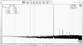
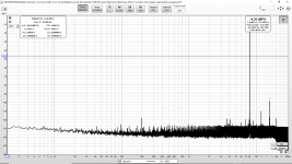
After my initial “quick” changes I have enclosed a sweep along with 1kHz and 8kHz spectrums.
This appears to be at the levels which signify the limits of my SB0490. About 100 dB down at 1kHz. I am sticking with 44.1kHz until I understand what is going on with 48kHz and 96kHz.
To measure lower distortion I will need to get a better audio interface/ADC working for measurement. Perhaps the Creative Professional/E-MU 1820 will allow me to do that later.
Note that the 3.66kHz spike is from the SB0490 and not the ES9038Q2M.
The initial “quick” changes are as follows:
The logic/objective of the Panasonic OS-CON ultra-low ESR capacitor usage is as follows: Attempt to prevent noise from noisy sources (such as 3.3V digital supply pins) from transferring over to sensitive analog pins. Since there are ferrite beads all over the board I thought I would try to use them to help prevent noise from the noisy sources from getting to the sensitive clock and analog pins. It is a little bit like two CLC filters between each noisy source and each sensitive supply pin on the board.
Considering the supply caps already on the power buss and the added OS-CON capacitors on the 3.3V supply buss it is a little bit like:
Noise Source > Low ESR OS-CON > Ferrite Bead > Power Buss & Existing Supply Capacitors > Ferrite Bead > Low ESR OS-CON > Analog Pins
Or a little bit like: Noise Sources > Shunt C > Series L > Shunt C > Series L > Shunt C > Sensitive Pins
At each sensitive analog pin there is now the stock ceramic decoupling/bypass capacitor, stock tantalum and now an added OS-CON 560uF 6.3V. That should provide a pretty decent upgrade over stock in terms of offering a solid low impedance across a respectable bandwidth. The combined three types of bypasses should result in a solid and respectably wide band low impedance now.
The Panasonic 6SEPC560MW OS-CON is rated 7mOhm in the datasheet. I freshly calibrated my meter to the socket interface using copper wire and when I measured this bag of 6SEPC560MW I read 3mOhm. On the AVCC pins I used two in addition to the stock 100uF 16V ELNA RA3 and stock (unknown) 1206 ceramic bypass. So perhaps around 1.5mOhm after the stock 4.7 Ohm 1206 resistor that is on the board between the 3.3V buss and each AVCC pins.
I am hoping that this is now a reasonably listenable initial configuration allowing me to work more leisurely on more substantial upgrades such as:
Notes on the cost of these modifications:
- 1kHz spectrum reads about 0.0012% for 2nd and 0.0010% for 3rd.
- The quick single sweep reads about 0.0020% for 2nd and 0.0019% for 3rd.
This appears to be at the levels which signify the limits of my SB0490. About 100 dB down at 1kHz. I am sticking with 44.1kHz until I understand what is going on with 48kHz and 96kHz.
To measure lower distortion I will need to get a better audio interface/ADC working for measurement. Perhaps the Creative Professional/E-MU 1820 will allow me to do that later.
Note that the 3.66kHz spike is from the SB0490 and not the ES9038Q2M.
The initial “quick” changes are as follows:
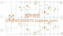
- Supply ONLY the output/op-amp with a discrete current source and shunt regulator (+/- 15V).
- Supply the LM7805 with a separate regulated 9.6V supply (from Digitech/Harman International for musical instrument signal processing equipment).
- Add one Panasonic 6SEPC560MW OS-CON 560uF 6.3V across all the stock 1206 ceramic bypass capacitors. Leaving the stock ceramic and tantalum on each pin.
- Add two Panasonic 6SEPC560MW OS-CON 560uF 6.3V for each AVCC pin leaving the stock 1206 ceramic bypass capacitors, stock 4.7 Ohm 1206 resistor and stock 100uF 16V ELNA RA3 in place.
- Add one 270uF 16V solid polymer capacitor (unknown brand, measured 4mOhm) to each op-amp supply pin. Leaving the stock bypasses in place.
- “Remove” the Vcc/2 “offset generator” from the output section (used for single supply operation) by placing copper wire shunts over the bypass capacitors. I want both sides of the output section connecting to the same ground specifically the ground plane on the board. I don’t want one side of each ES9038Q2M output pair connecting to a noisy virtual ground generated from the power supplies.
- “Remove” (short) the output capacitors using copper wire shunts. I have film capacitors in all of my amplifiers.
- Using LM4562 for output. That is presently my best dual op-amp.
The logic/objective of the Panasonic OS-CON ultra-low ESR capacitor usage is as follows: Attempt to prevent noise from noisy sources (such as 3.3V digital supply pins) from transferring over to sensitive analog pins. Since there are ferrite beads all over the board I thought I would try to use them to help prevent noise from the noisy sources from getting to the sensitive clock and analog pins. It is a little bit like two CLC filters between each noisy source and each sensitive supply pin on the board.
Considering the supply caps already on the power buss and the added OS-CON capacitors on the 3.3V supply buss it is a little bit like:
Noise Source > Low ESR OS-CON > Ferrite Bead > Power Buss & Existing Supply Capacitors > Ferrite Bead > Low ESR OS-CON > Analog Pins
Or a little bit like: Noise Sources > Shunt C > Series L > Shunt C > Series L > Shunt C > Sensitive Pins
At each sensitive analog pin there is now the stock ceramic decoupling/bypass capacitor, stock tantalum and now an added OS-CON 560uF 6.3V. That should provide a pretty decent upgrade over stock in terms of offering a solid low impedance across a respectable bandwidth. The combined three types of bypasses should result in a solid and respectably wide band low impedance now.
The Panasonic 6SEPC560MW OS-CON is rated 7mOhm in the datasheet. I freshly calibrated my meter to the socket interface using copper wire and when I measured this bag of 6SEPC560MW I read 3mOhm. On the AVCC pins I used two in addition to the stock 100uF 16V ELNA RA3 and stock (unknown) 1206 ceramic bypass. So perhaps around 1.5mOhm after the stock 4.7 Ohm 1206 resistor that is on the board between the 3.3V buss and each AVCC pins.
I am hoping that this is now a reasonably listenable initial configuration allowing me to work more leisurely on more substantial upgrades such as:
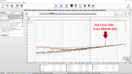
- Trying to make better 24-bit measures with Creative Professional/E-MU 1820
- Buying and trying out the new ultra-low noise TPS7A2033PDBVR
- Building op-amp style filters/supplies for AVCC
- Output section
Notes on the cost of these modifications:
- OS-CON 6SEPC560MW cost me 4.9 cents each
- Pictured discrete current source-shunt regulated supply was $9.16
- I already had the Digitech/Harman International supply but I think it cost $15 or something like that.
Attachments
-
 After Initial Changes 1kHz Sine Spectrum.png114.8 KB · Views: 232
 -
 Harmon HPRO 9p6 Regulated Supply.png956.9 KB · Views: 194
 -
 Class A Parallel Regulated Power Supply Schematic.jpg24.5 KB · Views: 146
 -
 Class A Parallel Regulated Power Supply.png365.1 KB · Views: 139
 -
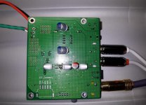 After Initial Modifications Back.jpg193.9 KB · Views: 243
 -
 After Initial Modifications Front.jpg184 KB · Views: 253
 -
 After Initial Changes Sweep - Copy.png221.3 KB · Views: 245
 -
 After Initial Changes 8kHz Sine Spectrum.png141.1 KB · Views: 253
Last edited:
regarding AVCC pin, would it be safe to assume that the stage being powered with that connection is drawing constant current, if it has been designed with minimal PSRR? any variation in voltage due to dynamic loading would then deteriorate significantly the performance. it would make the pool of candidate regulator much bigger...
More than 10 years ago, discussing ES9018 on this forum, it was proposed, that "DAC consists of 64 MOSFET switches, and each MOSFET switch has a resistance of 50k Ohms". I am not sure, whether there is more precise info available on this matter, but those switches are still switching for sure 😀
Eziitis,
It would be very nice if Pavel would retry that simulation of the LT3042, with 10uF output capacitance, instead of the simulated 470uF. It is not by accident that the producer strongly recommends that filter capacity value.
With 10uF we will get back the claimed min. 1Mhz bandwith, which dictates the response inside 1usec instead of the <<16usec claimed in the sim..
Could we say that maybe it had been set up on purpose..? No that cannot be. On a positive note I see that a minimum bias current of 60mA had been maintained, at least.
Otherwise the result, cca 10mohm output impedance is not that far from reality. I have measured cca 5mohm, or a bit better, with 1MHz bandwith. Rising to 20mohm at 2Mhz.
Question is, and I had already suggested it to You: an LT3042, VSON package, can be organized in cca 10mm*10mm area. Or less.. And so, some mm away from the Dac VREF pins.
How many mohm are say, 5cm pcb trace (not plane)..?
What does it worth, a theoretical uohm regulator, dozens of mm away from the load?
Ciao, George
Thanks, good point indeed. I know about the attempts to solder caps and regs directly on the DACs pins, sort of p2p with SMD parts. And the results seem to be good enough. Not very practical though.
More than 10 years ago, discussing ES9018 on this forum, it was proposed, that "DAC consists of 64 MOSFET switches, and each MOSFET switch has a resistance of 50k Ohms". I am not sure, whether there is more precise info available on this matter, but those switches are still switching for sure 😀
i'm certainely not a dac expert, but i would guess at least a part of the output stage is is constant current, because of the differential output signals.
I have heard that one technique to reduce noise (from switching currents in a DAC) is to always have the current flowing but you steer or direct (switch) the current between two paths one of which is the output. That way the total flowing current is much closer to constant and generates much less noise from switching.
I am certainly not an expert. And I don't know how it is done inside the ES9038Q2M.
Hopefully a more knowledgeable person can comment.
I am certainly not an expert. And I don't know how it is done inside the ES9038Q2M.
Hopefully a more knowledgeable person can comment.
does any kind soul have the ES9038PRO setup in a Protel/Altium Integrated library (schematic and footprint).
I'm using DXP 2004.
Thank you.
I'm using DXP 2004.
Thank you.
Kozard...
Did you measured noise on power supply with a scope to see what happened with adding so big caps. Put 1khz into digital input and measure what happenes.
My approach is bring as clean voltage as possible on the board and there some small and high quality caps. Pps, pml in small size because no space for big foil caps. Sunting noisy lines with big caps just supress noise into gnd. Pcb gnd is poor so noise is flowing all over the board and mix with other noises.Problem is that noise pass back to circuit trought caps and resistors... if board would be 5layer it will be much easier to filter noise. But noise and thd numbers are not all that matters. Choosing the right material brings own sound charracter of the Dac.Bypassing power sopply lines with ceramics or pps , pml gives different sound charracter.
does any kind soul have the ES9038PRO setup in a Protel/Altium Integrated library (schematic and footprint).
I'm using DXP 2004.
Thank you.
Sabre ES9038PRO + ES9311Q 8-Channel XLR/RCA Evaluation Board - Ismosys
1. download Evaluation Board Design Files
2. PCB is made in Diptrace. Install Diptrace Trial and export components/footprints from design cache
The boards schematic is in Orchad format, perhaps Altium could open it
Last edited:
Elaborate what? How output impedance relates to load transient? Simply the PS voltage variation to a load transient is its output impedance times the change in load current. You should take a second look at the Ohms law.
And this matters in general, not only for ESS DACs
The particular simulation was an example indicating that with “discrete” (an op amp anyway) design one can achieve better responses to a load transient.
Btw, that is the reason, why ESS reference designs used op amp buffer for AVCC, not LDO reg, until they designed their own ES9311
The simulation shows 10mA load variation from 60 to 70 mA at 50 kHz. Where exactly on the datasheet do you see that on AVCC?
But there is an easy way for you to support your statement. Please provide one measurement of an ESS dac with your discrete regulator. You can pick any standard measurement to your liking. Then it should be relatively easy to compare that measurement to ASR's measurements of a DAC with the same ESS chip but without discrete regulator. If what you state holds water there should be something visible of the claimed better performance of discrete regulator.
- Home
- Source & Line
- Digital Line Level
- ES9038Q2M Board