OS used cascode to allow lower voltage low noise transistors to be used in LTP.
OS removed mpsa18 from the BOM as some builders had problems with these transistors but if mpsa18s work fine in the other channel than something else is wrong.
From what you are saying problem is further down the line past q1-q8 transistors. Possibly bias transistor or drivers or even VAS or something in their circuits create problems. Did you measure each transistor and other components before soldering in? It saves a lot of troubles afterwards.
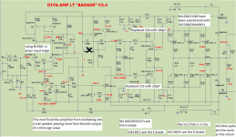
I have attached diagram with DC voltages and mods to remove oscillations one of our builders here had. This diagram was published some time ago. Measure DC voltages at these points as well as AC voltages (should be zero) on both boards and write them down. Problem is caused by some part/s behaving badly under DC so knowing where's the difference in DCs or AC apeares hopefully faulty parts can be roughly identified. AC can be very HF so good AC voltmeter or oscilloscope are needed but try with what you have.
cheers,
PS emitter resistors identified by OS have non-inductive version, zoebel resistor should be non-inductive or a few resistors in parallel used to reduce inductance but in your case problem is somewhere else or one of these resistors is not so good.
Did you inspect the problem board? Sometimes tiny crack or conductive "hair" joins tracks.
OS removed mpsa18 from the BOM as some builders had problems with these transistors but if mpsa18s work fine in the other channel than something else is wrong.
From what you are saying problem is further down the line past q1-q8 transistors. Possibly bias transistor or drivers or even VAS or something in their circuits create problems. Did you measure each transistor and other components before soldering in? It saves a lot of troubles afterwards.
I have attached diagram with DC voltages and mods to remove oscillations one of our builders here had. This diagram was published some time ago. Measure DC voltages at these points as well as AC voltages (should be zero) on both boards and write them down. Problem is caused by some part/s behaving badly under DC so knowing where's the difference in DCs or AC apeares hopefully faulty parts can be roughly identified. AC can be very HF so good AC voltmeter or oscilloscope are needed but try with what you have.
cheers,
PS emitter resistors identified by OS have non-inductive version, zoebel resistor should be non-inductive or a few resistors in parallel used to reduce inductance but in your case problem is somewhere else or one of these resistors is not so good.
Did you inspect the problem board? Sometimes tiny crack or conductive "hair" joins tracks.
Attachments
Sometime you spend more time searching for problem than just re stuffing another board or remove components from board and starting over. You have one good board so you do know what you are doing. Worked for me in the past after days searching for problem. Too good a project not to finish.
On the good channel, at the bases of q1 and Q2 I get -.83v. on the bad channel I get -.234v. I can't seem to track down where the difference is coming from. R6 has same voltage on the output side, -.3mv. bounces around on the bad channel a tiny bit as it is measuring DC offset, but ac there is negligible, 0.1mv.
Voltage drop across r14 is same for both, right around 8.25v. but voltage relative to ground for good channel is -9.1v on the CCS side, while bad channel reads -9.25v. both channels read 3.7ma per build guide.
Voltage drop across r14 is same for both, right around 8.25v. but voltage relative to ground for good channel is -9.1v on the CCS side, while bad channel reads -9.25v. both channels read 3.7ma per build guide.
Are voltages on bases of q1 and q2 identical?
I assume that transistors q1 to q8 are fine as you have replaced these (and checked before soldering in) as well as components (R, D, C) of their circuits.
Are voltages at other points further down identical? Where are the differences?
cheers,
I assume that transistors q1 to q8 are fine as you have replaced these (and checked before soldering in) as well as components (R, D, C) of their circuits.
Are voltages at other points further down identical? Where are the differences?
cheers,
I drill and tap my heatsinks myself and my usual 6/32 screws do not fit the transistors. What size do most use to attache the output transistors to the heatsink when drilling and taping the heatsinks themselves. I am thinking mm.
Thanks, I thought of 4-40 but was not sure if you could securely clamp down the transistors with them.
i do not tap my aluminum heatsinks, i use the screw itself, a self tapping screw works fine, drill the holes with 2.5mm bits and you are go....wd40 or a light machine oil...
I was poking around on my badger again, and I wonder if I may have come across an issue. Unfortunately, I was spoking around with a probe to read current , and slipped, and blew one of the vas transistors, q11. So I pulled it, figured I would pull all three, q10, 11, and 12, and I noticed the npn 3503 were d gain class, 80 to 120 hfe, and the pnp 1381 was e class, 100 to 200, so my gains were mismatched in the vas and the large CCS. Would this lead to my instability problem? I was going to order matching gain class replacements, but they don't seem to be available anymore. Should I just replace with mje340 and mje350? They seem to be available, but are 30to 240 hfe. I guess having good ovelap in the hfe might be important, and something my case CCS did not have. And I figure it might be good to replace the 3503 with mje340 as well. Barking up the wrong tree? Now I have two to fix. Gah.
The mismatched gains aren't really a problem. MJE340/350 aren't a very good choice for VAS transistors.
Yeah, I was looking at it, and the Vas is only on one side, made up of q9, a992, and q10, 1381. The q11 and 12 are the CCS, and so gain mismatch shouldn't matter. That makes sense.
I made progress. I believe my problem lies with q1 and Q2. I had a non matched pair of mpsa06 (can't remember gain class). I had 11 ohm base stoppers in place of the 2.2 ohm on the output devices. I replaced the q10, 11, 12, and 13.
I measured voltages against good channel (I fixed it and it is working fine) and mapped my progress across the schematic. Voltages really only varied At base of the input pair. So I stuck the matched mpsa18 back in there (good channel uses mpsa18), and the negative voltages on the bases of q1 and q2 dropped from -235mv at each, to -115mv on q1, and -175mv on Q2. Still not in spec, but significantly better. At full power from the wall, 110vac, amp was stable. Bias settled at 20.9mv. (I pulled bias trimmer and put fixed 300ohm resistor in place). Offset was ok around 3mv, but bounced around slightly in the 2.5 to 4mv range. Voltage drop across r14 was 8.2v for both channels.
Ok. Progress. So then I pulled the 10 ohm base stoppers at the output and replaced with 2.2 ohm per bom. Problem was back. Rapid runaway bias.
I'll post my voltage map in the morning.
So I am guessing I need a lower gain/better matched input device. Yay? Nay? Go start over?
you can match all npns and pnps' output trannies as a group, not with each other..
you can also increase the re to 0.47 ohms to prevent current hogging in case your beta spread at the output trannies is indeed wide....
raising re to 0.47 increases stability of bias but lowered re has lower distortion, so it is a compromise...
you can also increase the re to 0.47 ohms to prevent current hogging in case your beta spread at the output trannies is indeed wide....
raising re to 0.47 increases stability of bias but lowered re has lower distortion, so it is a compromise...
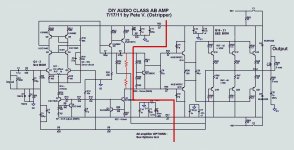
You got voltage mismatch on q1-q2 bases. It's source is either in ltp circuit (do you have resistor or zener there? are these grounded as in the first attachment?) or there's something wrong with your output like great hfe mismatch or oscillating driver. You may try to remove C6 (ideally should be non-inductive polypropylene).
Look at the second attachment and do this: desolder R31-32 (22ohm) on the power side. Remove q13 (bias) circuit and desolder R34-35 on one side just in case to disconnect drivers. Solder 1k resistors as shown in the attachment, apply voltage to ltp-VAS through R31-32 22 ohm resistors. If voltage on bases q1-q2 gets balanced then the problem is in the output, if not then the problem is in the ltp circuit. Source voltages look good to me, mirror voltages as well, similarly VAS. There are no miracles, one or more components are faulty somewhere.
cheers,
Attachments

Last edited:
Really? As increased balancing resistors' values yields to increased local NFB, I'd expect quite the contrary 😕?raising re to 0.47 increases stability of bias but lowered re has lower distortion, so it is a compromise...
Best regards!
- Home
- Amplifiers
- Solid State
- diyAB Amp The "Honey Badger" build thread