That's a multi-purpose table if there ever was one. Lunch, solder station, drinks, and amp building/testing. Gotta love it. 😉 What's that PCB under the cap bank? Is that part of the PSU? Is that a 3 or 4U case you're using?The Badger is alive! 🙂
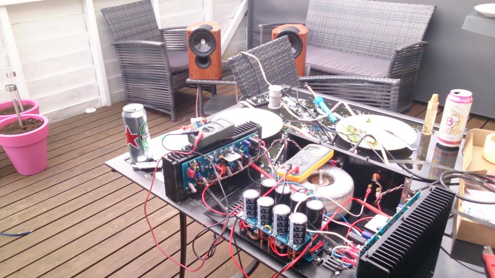
My wife wanted to sit outdoors and enjoy some drinks and bbq. Then the mail man showed up with New transistors for me, so I had to bring the amp out to keep my wife happy. I have had a lot of comments lately that I spend more time with my amp then with her. 😛
The PCBs below the caps are the rectifiers and soft start circuit. It's a 3u chassis.
The PCBs below the caps are the rectifiers and soft start circuit. It's a 3u chassis.
I also did the test with DMM and found it non conductive. But I suspect that a megger would give different results.
What's a "megger"?
Ron
What's a "megger"?
Ron
An insulation tester. It applies voltage (usually 300-1000v) to the test probes to measure resistance. You usually use it between the conductors in a cable to test for leak current and verify that the insulation is good.
You often get a different result with enough voltage to create arcs.
Last edited:
What's a "megger"?
Ron
The old day meggers were great fun. You get some sucker to grab the leads, you spin the crank and watch their hair stand up. It's a mega-ohm meter. The early designs used to produce high voltage with a hand crank to test insulation.
I had PC motherboards go up in smoke with arctic silver.
Do yer damn research .... there are many "versions" of this stupid
"bombed out compound". 😀
PS - yes, V5 is not fully conductive , every version is more/less
conductive. ZNO is not perfect , either. It is an insulator typically ,
but impurities and temperature keep it from being perfect , as well,
Still , better than AS5.
AS3 is a damn wire !!!
Edit - the compression of the compound is another big factor. PC cpu - less ..
a "cranked" output heatspreader bolt .... different.
OS
Last edited:
I had PC motherboards go up in smoke with arctic silver.Fool me once, shame on you...
Do yer damn research .... there are many "versions" of this stupid
"bombed out compound". 😀
Oh, someone's a little grumpy....
OS
Yes, I know it was a joke, so was my post.
🙂
Thanks for the explanation of a Megger, I remember having those in High School science class. Different name though.
Ron
Yes, I know it was a joke, so was my post.
🙂
Thanks for the explanation of a Megger, I remember having those in High School science class. Different name though.
Ron
I "grinned" .... just a straight answer. I sometimes just let it out.
Installed some wrong transistors. Well they be OK?
I accidentally purchased and installed some transistors which are similar to - but not exactly the same as - those listed in the BOM. Specifically, Q3 and Q4 in the cascode/current mirror and Q7 and Q8 in the VAS are supposed to be type KSC1845. I installed KSD1616A. They are both BJT NPN transistors. I have included a screen shot of the comparison of the two. My question is: Is it worth the effort to purchase and install the correct transistors?
Any help is appreciated! 😕
Attachments

They look good to me. I did not know about the 1616a.
As long as they are ECB , should be fine. Faster device (160mhz ft).
Cascode is the only pair that has to be >100V , beta helper in the VAS - also , >100v.
I actually use low voltage for my input pair (ksa/c -1015/1815) and current mirrors.
Input pair only sees @ 12-15V, current mirror just a couple. Cascode sees nearly the full rail.
OS
it appears to be a power transistor in a TO92 case. the capacitances and storage times will make it slower at the same current as KSC1845
I am a new diyer. In order to avoid the burn-out of the power transistors, I am thinking of testing the function of the whole circuit before soldering the power transistors into the PCB. Is it possible? If yes, what should be the correct reading across R36 or C20 if I feed a 1V signal into the input?
I am a new diyer. In order to avoid the burn-out of the power transistors, I am thinking of testing the function of the whole circuit before soldering the power transistors into the PCB. Is it possible? If yes, what should be the correct reading across R36 or C20 if I feed a 1V signal into the input?
I do that on all my amps. Just did my 4 slewmasters like that , 100%.
To do the badger , split R36 into two 68R -82R resistors in series. from the center
of the two , take R6's feedback signal. On the badger PCB , this would
just be as simple as each 68R soldered to the output rail.
What you have is a small amp , with just the drivers as outputs. read across Q14/15 (emitters)
for 1.2V and any output pair will be close to optimal bias. (don't forget to remove
the 68's and put in 150R - R36 , when done) .
Small heatsinks can temporarily be used on the drivers , BTW.
Edit - on mine , after this .... I just added 1 pair outputs , biased to perfection - then did the other 4 pairs
(5 pairs , all perfect).
OS
Last edited:
I'm planning to build a r2r attenuator to use with the honey badger. When calculating resistor values I need to know the input impedance for the amp. Is this R1 100k?
Separate power to Front end
I have been reading Honey Badger threads for what seems like days and have found answers to most of my questions, but have been unable to find definitive answers to these.
To provide a separate +/- 70V supply for the front end do I just remove R32/33 and apply the supply there? I am using a +/- 52V supply for the output stage.
Do these two separate supplies (separate transformers) share grounds at the board only?
I have lots of 2SK170's and would like to use these as the input pair. From what I have read I need to only change R15/16 from 100R to 10 to 22R. Is this correct? Do I need to change anything else? Would higher Idss be better in this application?
I have not read of anyone other than OS who has tried the JFET input pair. Has anyone else tried it?
Sorry for so many questions, but I thought I'd try to get as many as possible out of the way in one shot.
Regards.
Dan
The "boosted" supply thing is sort of a "chicken or the egg" type thing.
Let me explain -
Scenario 1 - output rails 60V , input stage 70V.
Badger reaches a 58.6V peak , output stage clips (and drivers possibly saturate).
Input stage is not clipping yet , but the saturated driver present a "wild" load
on the VAS (Q10/12).
Scenario 2 - Q10/12 (VAS) either clips at the same time or before the output stage.
In the simulator (heaven forbid !! 😛) ..... overall clip behavior seems better as
designed (lower input stage voltage). When the output stage clips independently ,
A much more "sticky , nasty" harmonic crunching waveform is created.
If the separate supply is passed through a capacitance multiplier and the output
is dropped slightly below the output rails , everything improves (psrr , overload).
If you want the OPS/IPS to both clip at the same time , nearly equal voltages.
A 70V supply (yes , just apply at R32/33 - remove) would give about 2V p-p
more out of the output stage ... that's all.
The Jfets , use 'em. remember the pinouts and the fact that the amp's closed
loop gain/gain margin will be reduced. actual gain will stay about the same. THD
will increase (2nd order will rise). Never ran long with Jfet's (mine were ewaste😱)
Did not fail , BTW.
OS
Thank-you so much OS. I will do as you suggest. Run the front end power supply through a capacitance multiplier, with the voltage a couple of volts lower than the output supply voltage.
And I will just use the JFETs. I am looking for a little more 2nd order distortion.
I am building two Badgers. I'll try one with JFETs and one with BJTs and compare. Thanks again.
Regards.
Dan
And I will just use the JFETs. I am looking for a little more 2nd order distortion.
I am building two Badgers. I'll try one with JFETs and one with BJTs and compare. Thanks again.
Regards.
Dan
- Home
- Amplifiers
- Solid State
- diyAB Amp The "Honey Badger" build thread