Hi Keantoken,
I'm just wondering which arrangement you think is best for the caps c116 & c114.
Above or below the main caps?
It's funny because almost every layout revision changes the nature of the parasitics here. Currently the long trace from the negative 100n pin to ground dominates it's loop inductance so the ringing doesn't appear on the rails but now it's ESL is probably larger than the lytics making it fairly useless. Not that it matters because the output transistors are all the way up in Canada. The only use for these capacitors is shunting RF noise from the input power and they perform that function best when they come directly after the power input terminals without any extra trace length.
I think Mark Whitney was worried about the rail impedance at the output transistors and the best way to address this would be a small lytic bypass to the ground side of the zobel from both rails.
If its below like in my last layout couldn't we just swap the speaker ground and the ground terminal and then run the traces like this to reduce the current loop.
That helps a lot, good thinking.
Last edited:
Question... Keantoken, please clarify
Were exactly do you want the G1 - G2 connection. Do you want it to connect directly to G1?
Were exactly do you want the G1 - Glift connection. Do you want it to connect directly to G1 or the speaker ground terminal?
Vargasmongo has the right idea in post 694, but the current arrangement probably wouldn't have any noticeable issue. Does G1 go to chassis or something?
I believe that G1 is just the designation for the Power ground and would of course go back to the 0v rail through the GND terminal on the main power supply board.Vargasmongo has the right idea in post 694, but the current arrangement probably wouldn't have any noticeable issue. Does G1 go to chassis or something?
Those two holes at G1 are just via's joining the copper top to copper bottom.
The other one is just for a test point.
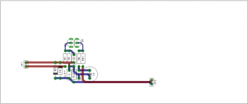
Like this
View attachment 946988
Last edited:
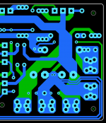
So something like this for the final version?Vargasmongo has the right idea in post 694, but the current arrangement probably wouldn't have any noticeable issue. Does G1 go to chassis or something?

So something like this for the final version?
View attachment 947015
That would help a lot with reducing the loop area.
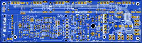
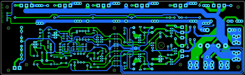
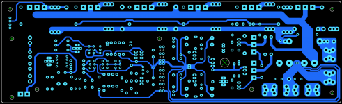
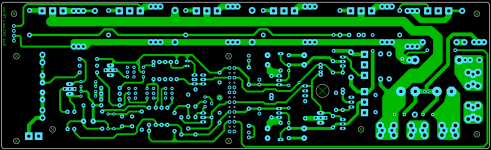
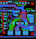
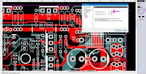
Based on all the comments and OS design intention this is the final version. Which optimizes the loop area given all other fixed constraints
Attachments
Last edited:
Based on all the comments and OS design intention this is the final version. Which optimizes the loop area given all other fixed constraints
Can the ground post be centered in between the +/-V?
stuart. You have moved one of the monting holes. So now i belive it do not line up with the predrilled UMS heatsinks.
Hi AudioSan. Yes your right I did move that mounting hole. That hole if I'm not mistaken was a additional hole added by OS to help with the load on the pcb when tightening the terminal screws. It is not part of the UMS and would have been needed to add anyway. To my understanding it's final position was not set in stone.stuart. You have moved one of the monting holes. So now i belive it do not line up with the predrilled UMS heatsinks.
If someone is unable to tap a hole they can use a plastic pcb stand off like the one shown.
Feel free to check the UMS and get back to me.

Based on all the comments and OS design intention this is the final version. Which optimizes the loop area given all other fixed constraints
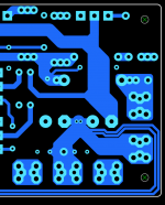
I wonder about the extra ground track for c114-116 to return to c115-117 ground pins. Why not just make it as short as possible accross the input terminals, as suggested in post #701 ?
Reading back over keantokens post I see what you're saying and what he was saying in that post but I guess I didn't pick up on it. I'll save another version make the changes and ask him again which version he prefers just incase I've missed something.I wonder about the extra ground track for c114-116 to return to c115-117 ground pins. Why not just make it as short as possible accross the input terminals, as suggested in post #701 ?
Thanks for the heads up. I guess I was just trying to mimic what OS had originally done.
Updated
Hi All,
Hopefully I have now interpreted Keantokens critiques.
I also had to update the SIP1 Protection Header as there was a creepage problem between the pins.
Keantoken, Please confirm this is correct. 😀
I wonder about the extra ground track for c114-116 to return to c115-117 ground pins. Why not just make it as short as possible accross the input terminals, as suggested in post #701 ?
Hi All,
Hopefully I have now interpreted Keantokens critiques.
I also had to update the SIP1 Protection Header as there was a creepage problem between the pins.
Keantoken, Please confirm this is correct. 😀
Attachments
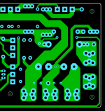

Another (very minor) thing. Is the wiggly track for nfb from the output to J3 really necessary ? Why not a simpler track to L1 pad ?
Edit: another thing: I'm not sure about the value of the spidery thing around G2. LED1, C101-102 could share a small local gnd plane without penalty at first sight, the same at the bottom of the board. Heck, you could probably connect C103 to it.
Edit: another thing: I'm not sure about the value of the spidery thing around G2. LED1, C101-102 could share a small local gnd plane without penalty at first sight, the same at the bottom of the board. Heck, you could probably connect C103 to it.
Last edited:
Hi,
i suggest again the protecting resistors for the bias TPs. It can be useful protection for peanuts.
Sajti
i suggest again the protecting resistors for the bias TPs. It can be useful protection for peanuts.
Sajti
Hi AudioSan. Yes your right I did move that mounting hole. That hole if I'm not mistaken was a additional hole added by OS to help with the load on the pcb when tightening the terminal screws. It is not part of the UMS and would have been needed to add anyway. To my understanding it's final position was not set in stone.
If someone is unable to tap a hole they can use a plastic pcb stand off like the one shown.
Feel free to check the UMS and get back to me.
View attachment 947187
Okei 🙂 I remember the same holes on the honey badger too, I've never used the UMS heatsinks, so don't know all those holes. I for one like to do my own drilling and tapping 🙂
Why does the feedback loop need to go through J3 and all around the world like that? why not go somewhere in between r113-c114 then R110 C115 instead and eliminate the outer trace and J3.
Also why not push down R111, J1,J2 to be at the same height of R112,113 and Q107 and fatten the output trace a bit? If Q105 is a problem you can prob reposition the whole ensemble down from Q105-c110 to C111-Q106 including the mid resistors.
Also why not push down R111, J1,J2 to be at the same height of R112,113 and Q107 and fatten the output trace a bit? If Q105 is a problem you can prob reposition the whole ensemble down from Q105-c110 to C111-Q106 including the mid resistors.
good idea R111 same high as R112 and R113 not sure what you mean about J1,J2
fatten output trace? but we have top and bottom copper already 4 oz of copper with both layers if the PCB is order as 2oz copper
1oz 10.2A 35u copper double layer makes 2oz so 20.4A example if order as 1oz
2oz 14.5A 70u copper double layer makes 4oz so 29A example if order as 2oz
fatten output trace? but we have top and bottom copper already 4 oz of copper with both layers if the PCB is order as 2oz copper
1oz 10.2A 35u copper double layer makes 2oz so 20.4A example if order as 1oz
2oz 14.5A 70u copper double layer makes 4oz so 29A example if order as 2oz
Attachments
- Home
- Amplifiers
- Solid State
- DIYA store "Wolverine" (Son of Badger) .... suggestions ??