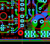
If you keep that layout and fix the feedback routing, C114 and C116 can go directly between the PSU terminals which can then be moved up. That will give room for the feedback traces. I would have the PSU traces travel together under the inductor and then diverge at right angles to reduce the loop area and keep it away from the inductor. The traces from lytics to power terminals can travel closer to the ground trace to reduce loop area.
Wow, this really snowballed. A lot of questions could be answered by looking at my loop area drawings and following the discussion.
I know this loop area stuff gets tiring after you have to scrap a few dozen layouts... But then the next board is much easier because you can plan around it from the beginning. A lot of this is improvised and made confusing because we are revising a PCB at the end of the process, which is generally bad for morale. Stuart is remarkably persistent but I can tell even he is reaching the end of his patience.
If you want low distortion at 20KHz full power, this is your labor of love.
We can think of an example. Imagine a 1 square inch current loop radiating to another 1 square inch current loop.
If the current loops overlap then there is 1:1 coupling. This means that the voltage which appears across the first current loop's inductance will also appear across the second current loop. If we overlap the current loops by half, then the coupling drops to 2:1.
When we reach the edge at 1" distance between centers, then our pickup loop occupies 1/8 of the immediate area around the radiating loop. So our coupling is something like 8:1. From there it follows inverse square law because outside the first loop, the field is no longer uniform.
The first layout was especially heinous because the feedback and lytic loops were largely overlapped, so we weren't even getting any benefit from the inverse square law.
At 10App sine output, then the PSU loop will be radiating something not entirely unlike a 5App 2nd harmonic. If we assume the inductance of the PSU loop is 22nH (probably wrong but in the ballpark), then going by inductive reactance the voltage across that loop will be 2pi*20KHz*22nH * 5A = 13.82mVpp.
With a 4ohm load, 10App equates to 80Vpp. So with full overlapping loops our THD would be something like 13.82mVpp/80Vpp=0.017%. If the current loops only touch edges then we reduce that by about 8, and get 0.0022% THD. Double that distance and it is reduced by another 4x which gives us 0.00055%.
At the input where any coupled distortion is increased by the amp gain, the distance requirement increases by sqrt(gain). So for a gain of 30, a 1" square input current loop would need to be 5.5x further from the PSU loop than the feedback loop is to have as little effect on the final THD.
Keantoken, would you share with us a PCB that you designed, built, tested and applied your distortion reduction techniques too...
If you keep that layout and fix the feedback routing, C114 and C116 can go directly between the PSU terminals which can then be moved up. That will give room for the feedback traces. I would have the PSU traces travel together under the inductor and then diverge at right angles to reduce the loop area and keep it away from the inductor. The traces from lytics to power terminals can travel closer to the ground trace to reduce loop area.
Wow, this really snowballed. A lot of questions could be answered by looking at my loop area drawings and following the discussion.
I know this loop area stuff gets tiring after you have to scrap a few dozen layouts... But then the next board is much easier because you can plan around it from the beginning. A lot of this is improvised and made confusing because we are revising a PCB at the end of the process, which is generally bad for morale. Stuart is remarkably persistent but I can tell even he is reaching the end of his patience.
If you want low distortion at 20KHz full power, this is your labor of love.
We can think of an example. Imagine a 1 square inch current loop radiating to another 1 square inch current loop.
If the current loops overlap then there is 1:1 coupling. This means that the voltage which appears across the first current loop's inductance will also appear across the second current loop. If we overlap the current loops by half, then the coupling drops to 2:1.
When we reach the edge at 1" distance between centers, then our pickup loop occupies 1/8 of the immediate area around the radiating loop. So our coupling is something like 8:1. From there it follows inverse square law because outside the first loop, the field is no longer uniform.
The first layout was especially heinous because the feedback and lytic loops were largely overlapped, so we weren't even getting any benefit from the inverse square law.
At 10App sine output, then the PSU loop will be radiating something not entirely unlike a 5App 2nd harmonic. If we assume the inductance of the PSU loop is 22nH (probably wrong but in the ballpark), then going by inductive reactance the voltage across that loop will be 2pi*20KHz*22nH * 5A = 13.82mVpp.
With a 4ohm load, 10App equates to 80Vpp. So with full overlapping loops our THD would be something like 13.82mVpp/80Vpp=0.017%. If the current loops only touch edges then we reduce that by about 8, and get 0.0022% THD. Double that distance and it is reduced by another 4x which gives us 0.00055%.
At the input where any coupled distortion is increased by the amp gain, the distance requirement increases by sqrt(gain). So for a gain of 30, a 1" square input current loop would need to be 5.5x further from the PSU loop than the feedback loop is to have as little effect on the final THD.
Thanks for the very interesting explanation!
QUOTE=Krisfr;6637607]Keantoken, would you share with us a PCB that you designed, built, tested and applied your distortion reduction techniques too...[/QUOTE]
And how that would help with this thread???
And how that would help with this thread???
Wow, this really snowballed. A lot of questions could be answered by looking at my loop area drawings and following the discussion.
I'm digging hard for either real world examples of KT's advice or any layout
tutorial covering this.
OS
At 1KHz my THD figures in the example would be 20x lower, so no one designing for 1KHz figures would probably notice unless their layout was particularly bad. And even if not their THD at 20KHz was probably equal or larger than the contribution of their layout. So I think this is Star Trek territory, we're going where no one's gone before... Except some people we don't know and who won't talk to us.
There are some class A amps that approach this but class A doesn't have to deal with the output switching situation.
I don't take your statements lightly, so here is what I suggest. Let's find someone who is good at math to check out my example. I put on a good show, but I'm really not good at math.
I thought I saw a tutorial on how to calculate the coupling between loops of wire in a PCB context, but I didn't find it. For all the discussions I found, even estimating it was too much for the participants, so FEMM was suggested and then no one bothered to comment after that. So I came up with what I know from my own research and reasoning.
Keantoken, would you share with us a PCB that you designed, built, tested and applied your distortion reduction techniques too...
I would have shared them here from the beginning, but I seem to have a need to eat, and I do hope to make money with my skills, someday...
Thank you , KT and Stuart....
Re -read both Self and Cordell books (Layout/distortion mechanisms) ,
Lots of "fringe" loop area layout techniques from TI and other manufacturers.
Yes , even after adding high- end or any reverse engineering to this research ,
I'm hard pressed to find ANY kit or OEM that is in this "star trek" territory.
I now believe , and I like being triggered into another learning curve.
Some ("who we don't know , or won't speak to us") Have PM'ed me.
We are REALLY on the right track. Some even explained the math to me.
Cool !
OS
Hi Guys,
What do you think about this possible solution.
It's not finished yet but it shows how to NFB trace routes a better path while still keeping the loop area low.
Keantoken and OS please comment so I can finish tiding up this tomorrow.
Just give R112 a little more space away from the big cap.
Nice !!
OS
I now believe , and I like being triggered into another learning curve.
Some ("who we don't know , or won't speak to us") Have PM'ed me.
We are REALLY on the right track. Some even explained the math to me.
Cool !
OS
Aw, now I feel like I'm missing out. 😀
Maybe if they anticipate their private knowledge to become known by the public, they are more likely to share with us.
I think you guys are breaking new ‘star trek’ ground here with this layout. The pathological focus on loop areas is absolutely critical to reduce distortion - I’ll admit my boards are nowhere near the level of attention to this aspect displayed here. A seriously good effort IMV.
Quick experiment to consider (I’ve tried it). Take a pair of 32 ohm headphones and clip a croc clip between the tip and ring. Drive your amp at close to full power into a load at say 1 kHz. Move the croc clip loop around near the amp board and the transformer. Around the transformer you will hear the hum/buzz from the radiated field (it will drop off perceptibly if you remove the input stimulus). On a bad amp layout, you will hear hash when you place the croc clip loop over the amp module.
Quick experiment to consider (I’ve tried it). Take a pair of 32 ohm headphones and clip a croc clip between the tip and ring. Drive your amp at close to full power into a load at say 1 kHz. Move the croc clip loop around near the amp board and the transformer. Around the transformer you will hear the hum/buzz from the radiated field (it will drop off perceptibly if you remove the input stimulus). On a bad amp layout, you will hear hash when you place the croc clip loop over the amp module.
Stuart,
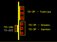
I believe you have control of board right now. Check the dimension of Q107/Q108 from the center of the lead or the center of the thru hole to the back of the package where it interfaces with the small heatsink.
For TO-3P from center of the lead to the back of the package
-Onsemi is 1.7mm nominal (NJW0281/0302 - what is called out on the schematic)
-Sanken is 1.7mm nominal
-Toshiba is 3.1mm nominal
Q107 and Q108 have to sit flush to the board for Q103's lead to protrude through the bottom of the board because of this Q107 and Q108 are "fixed" in there position.
Edit: Better use the max dimension
For TO-3P from center of the lead to the back of the package
-Onsemi is 1.9mm max (NJW0281/0302 - what is called out on the schematic)
-Sanken is 1.9mm max
-Toshiba is 3.3mm max
Jeremy
Last edited:
Stuart,
I believe you have control of board right now. Check the dimension of Q107/Q108 from the center of the lead or the center of the thru hole to the back of the package where it interfaces with the small heatsink.
For TO-3P from center of the lead to the back of the package
-Onsemi is 1.7mm nominal (NJW0281/0302 - what is called out on the schematic)
-Sanken is 1.7mm nominal
-Toshiba is 3.1mm nominal
Q107 and Q108 have to sit flush to the board for Q103's lead to protrude through the bottom of the board because of this Q107 and Q108 are "fixed" in there position.
Edit: Better use the max dimension
For TO-3P from center of the lead to the back of the package
-Onsemi is 1.9mm max (NJW0281/0302 - what is called out on the schematic)
-Sanken is 1.9mm max
-Toshiba is 3.3mm max
Jeremy
Thanks for looking into that Jeremy,
Currently the centers are ~6.8mm between the center of the leads on Q103 to the Center of the Leads on Q108.
If we go with your Max numbers of 3.3Max and then 1.2mm for the heatsink plate and a further 1.2mm for the MJE340 we end up at 5.7mm.
I calculated the vertical center height using the MAX dim for the NJW0281 (18.8mm) and the MIN for the MJE340 including leads using the Min dimension for the lead leg length and I get ~21.4 so there is about a 2.6mm overlap if the PCB is 1.6mm so it will be tight as you said. But the legs probably won't be at the minimum so it should work.
It would appear that the centers could be reduced by 1mm for Q103 to Q108 Center to center.
Attachments
Private IP ??
Barcasti , Goldmund , and older Luxmans.
I had to go private ways to get schema/layout info here.
Yup , at this level ... loop area considerations.
So , 15K$ to 45K$ !! before you see "star trek" ??
I am pleasantly surprised to see familiar IPS's driving these monsters.
The Bercasti M15 is a "spooky". Hawksford VAS is in there , too.
The 45K luxman is my "kypton" , a 2 stage LTP "insane" IPS.
Nope , no 1150W at 2R for the Wolverine ......
OS
Thanks for looking into that Jeremy,
Currently the centers are ~6.8mm between the center of the leads on Q103 to the Center of the Leads on Q108.
If we go with your Max numbers of 3.3Max and then 1.2mm for the heatsink plate and a further 1.2mm for the MJE340 we end up at 5.7mm.
I calculated the vertical center height using the MAX dim for the NJW0281 (18.8mm) and the MIN for the MJE340 including leads using the Min dimension for the lead leg length and I get ~21.4 so there is about a 2.6mm overlap if the PCB is 1.6mm so it will be tight as you said. But the legs probably won't be at the minimum so it should work.
It would appear that the centers could be reduced by 1mm for Q103 to Q108 Center to center.
Good.
The Q108/103 mating is what makes this EF3 excel thermally. Almost as
good as those thermaltrak special outputs.
OS
Stuart,
Q107 and Q108 have to sit flush so the leads can't move to shore up gap between the transistor and the small heatsink. Q103 and the small heatsink will be pulled toward Q107 and Q108 when the mounting screws are installed, then will Q103 leads be long enough?
I positioned Q107 and Q108 at 3.3mm for Toshiba, Onsemi, and Sanken between the center of the leads to the small heatsink. Maybe the picture illustrates what I'm saying better.
This means you have to move the thru holes for the transistor leads for the Onsemi and Sanken parts to 1.9mm center of leads to the small heatsink.
Correct me if I'm wrong or If you have another idea. Get a thicker small heatsink maybe?
Jeremy
Attachments
Last edited:
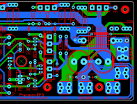
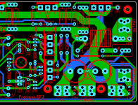
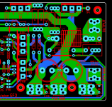
Board Options
Hi OS,
I am submitting these 4 boards for your direction.
I saved them a 2.1, 2.2, 2.3 and 2.4 to help keep the development separate.
The filename of the images below shows the version number
Notes...
Version 2.1:
Is one that I created after KT loop area comments. But you had some concerns about the NFB near the inductor.
Version 2.2:
Is the one that I did yesterday to try mitigate those issues but still had the loop area problem as in the earlier versions.
Version 2.3:
Is one I created this morning to try and solve the issue in version 2.1 but unfortunately I had to mess up the UMS again. So it was back to the drawing board to ensure it meets the UMS.
Version 2.4:
I think is the best version so far and is the one I hope that we can move forward with. It addresses the issues in Version 2.1 and also KEEPS all of the mounting holes from the UMS.
OS please advise if you are happy to move forward with Version 2.4.
I've e-mailed it to you.
Attachments
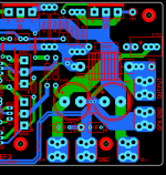

2.4 looks good.
I wonder whether KT could comment on what effect having C114/116
out at the terminals would be ?
The .1uF's in parallel with the lytics' = lower Z @ HF , should not matter
where exactly they are located.
Edit - C115/117 polarity is reversed.
OS
I wonder whether KT could comment on what effect having C114/116
out at the terminals would be ?
The .1uF's in parallel with the lytics' = lower Z @ HF , should not matter
where exactly they are located.
Edit - C115/117 polarity is reversed.
OS
Last edited:
I wonder whether KT could comment on what effect having C114/116
out at the terminals would be ?
That's what KT suggested in post #743
where exactly they are located.
Edit - C115/117 polarity is reversed.
Yes, your right..... super fast pick up.
Well done OS.
I just e-mailed you the 2.4.0 file
Attachments
Last edited:
- Home
- Amplifiers
- Solid State
- DIYA store "Wolverine" (Son of Badger) .... suggestions ??