I find this final schematic splendid and will surely build it but I need some special information:
In the offset control circuit, what is the function of the four 1N4148 diodes D4 D5 D6 D7 ?
Best
In the offset control circuit, what is the function of the four 1N4148 diodes D4 D5 D6 D7 ?
Best

good idea R111 same high as R112 and R113 not sure what you mean about J1,J2
the J1 J2 linkers. It doesn't matter hyow many amps it can take, unless other considerations are at work like they say...more is plenty. 😉
Based on all the comments and OS design intention this is the final version. Which optimizes the loop area given all other fixed constraints
At least you considered that.
While I agree/respect KT's accessment , The UMS screwup and the crazy traces
are "out there".
The V1.64 layout , all holes are present on the store heatsink. Triple checked !!
Perhaps , the Slewmaster way would be best.
Use the shielded wire from ops to ips nfb.
Why do I say these traces are "out there" ??
1. I can't find anything like this in my amp schema collection (PCB's).
Most japanese OEM's , No refined grounding layout other than the
basic power star decoupling.
2 . Looking at the Pass X150 and others , Pass pulls the NFB through a
ribbon cable. NFB is spaced within the ribbon , no associated NFB ground
return.
Looking at the real world HK amp I have , NFB(center point) ... snakes
through the input stage . IPS on the HK uses a tap from the main power
star (G1). NFB is in close proximity to the IPS ground return (G2)for a short distance.
HK seems to have a more refined grounding than the Pass scheme.
I feel we can do better than either.
Ideas or comments on the slewmaster shielded NFB return ??
OS
The Slewmaster wire thing worked but I was always concerned what would happen if it somehow managed to get disconnected. I'm curious how much of an issue the whole loop area thin is? There's no real current flow on the NFB trace, how much can it emit?
The UMS screwup
OS
Hi OS, I hope things are going well for you at the moment.
Regarding the UMS, Please read post #711 at it hasn't changed.
The UMS on this version 1.91 is still the as the UMS on 1.6.4.
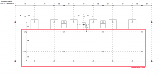
The hole near the terminal screws in the lower right corner of the board was not part of the UMS anyway. It would have been needed to added as you said.
To my understanding it's final position was not set in stone.
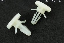
If someone is unable to tap a hole, they can use a plastic PCB stand off like the one shown in the attached image.
Attachments
Ideas or comments on the slewmaster shielded NFB return ??
OS
I see no reason why what other manufactures have done has to be the way we move forward with this layout. They may have made these choices for economic and rapid assembly reasons.
As we are using the DIP header then people who build this board have a choice, they can.
1. Run a shielded wire and not connect the jumper across the NFB header pins.
2. Connect the jumper across the NFB pins and not run the shielded wire.
It will be a good test for me to confirm using my distortion analyzer.
Then we will know for sure.
Either way I believe that we can still move forward with this current layout as it addresses those loop area issues KT raised, and to be honest I've spent more that enough time on this project.
That hole was in the UMS system. It's one of the transistor mounting holes.
Your right I double checked it and I didn't realise that the transistor mountings were included in the UMS and I had it upside down. 😱😱😱
It not a problem though as we can put the hole back and still make it work. 😀😀😀
See attached
Attachments

Last edited:
The hole on the lower right IS a UMS hole !! Badger has it.
As far as the loop area of the NFB , I just pointed out that even high end
OEM's came to the same conclusion as JW that the end tests reveal nothing
gained.
VZ audio and the slewmasters were tested. Spooky servo issue is the only one
I know about.
I'm still searching for a audio NFB loop area example , or even a paper on the
subject. all I find is RF and mixed signal layout ground returns and loops.
OS
It might be fun to test a couple different layouts and see if there's a measurable difference. No harm in trying it. I have a RTX6001. If there's a difference it will show it.
The Slewmaster wire thing worked but I was always concerned what would happen if it somehow managed to get disconnected. I'm curious how much of an issue the whole loop area thin is? There's no real current flow on the NFB trace, how much can it emit?
Inductance .... Self's book outlines inductance as a result of the large NFB loop
area issue.
He gives an example of the worst case (nano henry's). Of course , I simulated
with as much as a microhenry - not much PPM degradation. But , a slight shift
in the phase margin.
OS
The loop area for the NFB shouldn't be as much of a concern as the output stage which has alternating half sine wave currents flowing but it's more important not to route the NFB by those or any sources of noise. The NFB will be low impedance until it goes through the feedback resistor, after which the impedance goes high and becomes way more susceptible to noise.
Also the missing screw was adding mechanical stability in the corner where all the wire connections are.
Also the missing screw was adding mechanical stability in the corner where all the wire connections are.
Last edited:
The hole on the lower right IS a UMS hole !! Badger has it.
OS
Its fixed now and restored to its original location.
The loop area for the NFB shouldn't be as much of a concern as the output stage which has alternating half sine wave currents flowing but it's more important not to route the NFB by those or any sources of noise. The NFB will be low impedance until it goes through the feedback resistor, after which the impedance goes high and becomes way more susceptible to noise.
Also the missing screw was adding mechanical stability in the corner where all the wire connections are.
That is why I kept NFB (low z) away from anything , and transitioned to
the FB resistor (and the TMC FB) right at the IPS.
I'm digging hard for either real world examples of KT's advice or any layout
tutorial covering this.
I've found (in the chip amp world) , soldering the FB resistor right across
the pins of the chip and mentioning the loop area consideration. Still can't
find this at the "big amp" level.
OS
Small looparea also lowers the amount of pickup from sources that cause humm and other noise.
In my previous post, you can see that I joined the input and fb loops at Rlift. No mixing of the two signals allowed.
Most of the influences of layout are difficult to simulate. All you can do is practice best layout techniques.
In my previous post, you can see that I joined the input and fb loops at Rlift. No mixing of the two signals allowed.
Most of the influences of layout are difficult to simulate. All you can do is practice best layout techniques.
I have nothing against input caps but know that these can leave a strong signature in the final presentation.
IMO a good way to "open" industrial caps like the wimas is to bypass them with a small silver mica or styroflex.
For 10uF a small 15p or 20p SM is good.
Maybe you could leave space for a small bypass cap in the input.
IMO a good way to "open" industrial caps like the wimas is to bypass them with a small silver mica or styroflex.
For 10uF a small 15p or 20p SM is good.
Maybe you could leave space for a small bypass cap in the input.
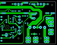
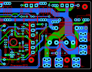
Possible solution,
Hi Guys,
What do you think about this possible solution.
It's not finished yet but it shows how to NFB trace routes a better path while still keeping the loop area low.
Keantoken and OS please comment so I can finish tiding up this tomorrow.
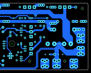
Hi Guys,
What do you think about this possible solution.
It's not finished yet but it shows how to NFB trace routes a better path while still keeping the loop area low.
Keantoken and OS please comment so I can finish tiding up this tomorrow.
Attachments


- Home
- Amplifiers
- Solid State
- DIYA store "Wolverine" (Son of Badger) .... suggestions ??