Yes, PSU ground and feedback ground for the frontend share the same conductor, I mentioned this earlier. The main offenders in terms of distortion currents is the predriver lytics.
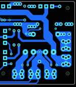
Here is some drawings of the current loops.
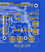
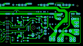
First picture is the current loops for the PSU caps and the PSU input. These are the areas where the rectified OPS currents have been physically separated, so they radiate strong even harmonics. At HF the total loop area decreases because the capacitors shunt some of the current.
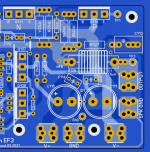
Second picture shows the feedback current loop. Notice that it entirely overlaps the capacitor current loop. Overlapping loops have 100% coupling. This means that the voltage that appears across the inductance of the capacitor loop will be coupled to the feedback signal at a 1:1 ratio. The areas that don't overlap couple according to the inverse square law and their distance to the offending current loop.
3rd picture shows an alternate feedback route that eliminates almost all the loop area, but will probably require a jumper, and it would help to turn the PSU terminals 90 degrees.
Thanks for the input KeanToken, It certainly makes sense. I am having ago at making those changes as you suggest. I'm not sure if I'll be able to do it, but its worth a shot.
The terminal screw macro was a little out so I measured an actual one I have and tweaked the macro.
Attachments
Yes, PSU ground and feedback ground for the frontend share the same conductor, I mentioned this earlier. The main offenders in terms of distortion currents is the predriver lytics.
Can you possibly draw a basic sketch of how you may run the trace.
The feedback ground should run with the feedback trace through it's whole length, from the groundlift all the way to the output ground. G2 can run to G1 like it does already, but without joining the feedback ground trace, it can run beside it.
What is the mouser page for the output/PSU terminals?
What is the mouser page for the output/PSU terminals?
Hi ST I found that C3 was a little offset I just adjusted since the pitch is 2.5mm y divided by 2 and give me 1.25 mm then I center the silkscreen using 3 silkscreen to center out between the pads accurately 
Attachments


Also, C114 and 116 look wrong and should be placed closer to the output devices.
At the input is a good position for these capacitors as their resonance will form a notch filter rather than a resonant booster. For the output devices, a 22uF capacitor across the rails at each device will clean up some resonant modes.
Perhaps, swap the place of the power and output on the board.
That would be good if it makes the layout less of a pretzel. It would make the feedback pair less snaky. But with the new feedback routing there may not be much to gain except for a different looking layout.
What other parts of the circuit need to have low inductance?
It just depends on what currents are flowing and what potential capacitances there are to resonate with. Output transistors are fairly capacitive, so reducing inductance in the collector-ground run helps. The frontend is more tolerant to inductance because the capacitances are lower. The input current loop could pick up some radiated harmonics but the loop area is not really that bad there.
That's what looks like will work the best.Perhaps, swap the place of the power and output on the board.
But for now, I have done it without doing that but had to rotate C114
If OS is OK with me swapping the terminals I'll have ago at that tomorrow.
Please advise OS
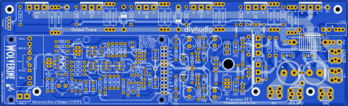
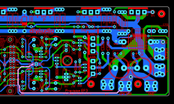
This is what I have so far.
I'll check out your other notes then. That wasn't easy.
I have kept a minimum of 1.5mm between traces and 2.25mm between terminals or Terminals and other traces.
Attachments
Last edited:
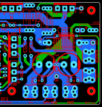
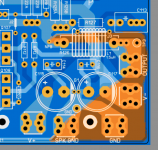
Here are the input and feedback loops in the frontend. Notice the signal and ground traces cross in the middle so you get a sort of figure 8 shape. With my suggestions in post 684 you would be removing the trace that goes from G2 to the groundlift resistor.
Attachments

I will be happy to be a guinea pig by ordering up some boards and building one once it is final final final... 🙂
Here are the input and feedback loops in the frontend. Notice the signal and ground traces cross in the middle so you get a sort of figure 8 shape. With my suggestions in post 684 you would be removing the trace that goes from G2 to the groundlift resistor.
Hi KeanToken, Please review the PCB and check my interpretation of your notes is correct. Thank you for taking the time to prepare those images on the loop area they really helped to understand your explanation.
Attachments


Last edited:
Hi KeanToken,
Sorry for all the updates, but I like to focus on one thing at a time.
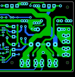
I managed to reduce the G2 Loop area.
If you can check this version and give feedback that would be awesome.
Sorry for all the updates, but I like to focus on one thing at a time.
I managed to reduce the G2 Loop area.
If you can check this version and give feedback that would be awesome.
Attachments

Hi KeanToken,
I re-read over your posts and saw that your preference was to have the input caps C114 & C116 located at the PSU input.
So I've done a version with them at the input.
Take a look between the two version and let me know which is your preferred layout.
I re-read over your posts and saw that your preference was to have the input caps C114 & C116 located at the PSU input.
So I've done a version with them at the input.
Take a look between the two version and let me know which is your preferred layout.
Attachments

Hi ST yes that looks good hey I was thinking about those traces the two that are connected to SPK GND I think this will be best I mean of course if this is approved by OS, a wire can be run from that GND pad to PSU GND that will be better I think too much maybe? 😛
ST I attached the file with that change here 🙂
ST I attached the file with that change here 🙂
Attachments

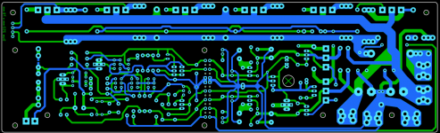
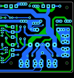
The output current loop now looks like this. It is mainly the distance between the output and ground terminals that is opening up the current loop. For instance, if you pulled the output wires to the corner of the board and joined them over the feedback trace, you would close the current loop. The arrangement in post 687 was better.
The new grounding looks good to me.
The new grounding looks good to me.
Attachments

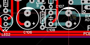
Hi Keantoken,The output current loop now looks like this. It is mainly the distance between the output and ground terminals that is opening up the current loop. For instance, if you pulled the output wires to the corner of the board and joined them over the feedback trace, you would close the current loop. The arrangement in post 687 was better.
The new grounding looks good to me.
I'm just wondering which arrangement you think is best for the caps c116 & c114.
Above or below the main caps?
If its below like in my last layout couldn't we just swap the speaker ground and the ground terminal and then run the traces like this to reduce the current loop.
The last layout I did has the advantage that all screw thermals run to the main capacitors or G1 using top and bottom copper layers.

I guess that you could also rotate that terminal and place it at the edge of the board like the -v and the outputThe output current loop now looks like this. It is mainly the distance between the output and ground terminals that is opening up the current loop. For instance, if you pulled the output wires to the corner of the board and joined them over the feedback trace, you would close the current loop. The arrangement in post 687 was better.
The new grounding looks good to me.
And put the mounting hole back were it was before

- Home
- Amplifiers
- Solid State
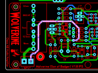
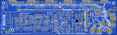
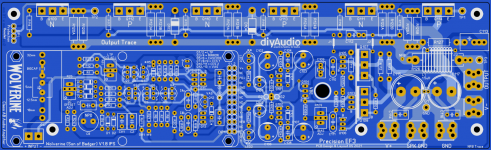
- DIYA store "Wolverine" (Son of Badger) .... suggestions ??