If you read back through the thread Pete made some recommendations for resistors. Dale/Vishay CFP2 resistors will fit.
Please post a link to the datasheet.If you read back through the thread Pete made some recommendations for resistors. Dale/Vishay CFP2 resistors will fit.
I still think that we need more than 1 option. Aren't those resistors very expensive as well and we need 12 of them.
Dale CPF2 have a smaller body than almost every other 2W. They are not always easy to find and should not be used as a reference size, although being nice resistors.
Standard 2W or 3W metal film resistors should be specked even if it's with there legs tightly bent.
Standard 2W or 3W metal film resistors should be specked even if it's with there legs tightly bent.
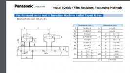
Here's the datasheet. https://www.mouser.ca/datasheet/2/427/cpf-1762878.pdf Check out Panasonic's recommendation for insertion. Almost anything will go.
Attachments
Resistors ??
https://www.mouser.com/ProductDetail/Welwyn-Components-TT-Electronics/WP2S-R47JA25?qs=sGAEpiMZZMtTURnxoZnJAPvElaXTPdXTKl0Wt8%2FIHcH9gxJ1FFtgng%3D%3D
Cheep !! 😀
Edit - Vishay military - https://www.mouser.com/datasheet/2/427/rwmilita-1762480.pdf
Seems to be many SMD wirewounds. Hmmm ... 13.5mm length.
SMD pads for R120 - R125 ??
https://www.mouser.com/ProductDetail/TE-Connectivity-Holsworthy/SMW2R47JT?qs=sGAEpiMZZMtTURnxoZnJAG%2FCFWXYTHFRsA%252BaLOsAlwE%3D
OS
Last edited:
I would have thought that 3w would be the bare minimum.
Considering 3 transistors into 4 ohms with 60v rails.


I would have thought that 3w would be the bare minimum.
Considering 3 transistors into 4 ohms with 60v rails.View attachment 946434View attachment 946435View attachment 946436
60V 4ohms, and 3 pairs means 5A peak current/device, and only half cycle. The means 1.6A continous, which is 0,56W for each 0.22ohms.
(Edited, because my mistake)
Sajti
Last edited:
Ok.. I see my mistake. Thanks guys.Yup ...
I still like the 3W route for 4R. Plenty of either SMD/TH at mouser.
OS
But I guess the question remains.
Should we consider moving the top of the pcb up 4mm to make it the same 10mm overlap as the bottom is and increase the space a little more.
It wouldn't take long to adjust the pcb.
Last edited:
You will have to look to the suggested output device mounting on the UMS spec.
You will want to have sufficient lead length between the PCB OP holes and
and the UMS heatsink holes. Try to stay with the original Badger spacings.
Those are highlighted in the UMS PDF.
OS
You will want to have sufficient lead length between the PCB OP holes and
and the UMS heatsink holes. Try to stay with the original Badger spacings.
Those are highlighted in the UMS PDF.
OS
Last edited:
I made mistake with the calculation (forgot half cycle), so 0,56W for 0.22ohms.
Sajti
So 2W devices are quite valid , as well. Good. Most 2W's are 10-12mm.
OS
Please Review
Hi OS,
I believe that Harry is just about done with the BOM review and I have been making a few changes as he has been checking. He found a body length problem with the silkscreen and pads for most of the diodes. So I have redrawn and adjusted accordingly.
Please review what I have done.
Hi OS,
I believe that Harry is just about done with the BOM review and I have been making a few changes as he has been checking. He found a body length problem with the silkscreen and pads for most of the diodes. So I have redrawn and adjusted accordingly.
Please review what I have done.
Attachments
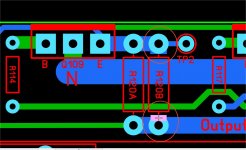
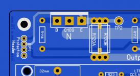
SMD option for R120-125
Small square pads (circled) will also give the option -
Moulded SMD wirewounds.
https://www.mouser.com/datasheet/2/418/5/ENG_DS_1773242_F-720908.pdf
If I could find the SM-5 varient - digikey has them.
Blocked
.93c X 6 - very cheap.
Talk about a non-intrusive emitter resistor. 🙂
edit - or ... make that center emitter resistor through-hole into the SMD pads. Don't be scared
of these SMD's , they are huge (7.3mm X 13.5mm).
OS
Attachments
Last edited:
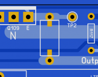
Hi OS,
I'm not sure that's going to work.
The metal lead / strip that you solder to under the resistor encroaches in the creepage allowance.
The inside of the lead / strip measures 8.6mm
I removed R120A / R120B for clarity.
This might be a good choice.
PNP300JR-73-470R
or
WNC470FE
I'm not sure that's going to work.
The metal lead / strip that you solder to under the resistor encroaches in the creepage allowance.
The inside of the lead / strip measures 8.6mm
I removed R120A / R120B for clarity.
This might be a good choice.
PNP300JR-73-470R
or
WNC470FE
Attachments
Last edited:
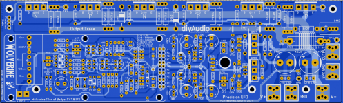
DIYAWolverine1.8 Final
Hi OS,
I'm done.
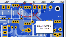
I managed to increase the emitter resistor lead pitch from 16.25mm to 18.5mm with a little tweak to the output trace. This will hopeful give more people more options to use parts that they have or are able to source locally were they live.
I hope you like it and approve this fine PCB for manufacture.
I suggest that someone else does a final schematic to pcb trace check to ensure that the circuit has been routed correctly.
PS. The resistor above were 470 ohms sorry about that. But equivalent 0.47 or 0.5 ohms are available.
Hi OS,
I'm done.
I managed to increase the emitter resistor lead pitch from 16.25mm to 18.5mm with a little tweak to the output trace. This will hopeful give more people more options to use parts that they have or are able to source locally were they live.
I hope you like it and approve this fine PCB for manufacture.
I suggest that someone else does a final schematic to pcb trace check to ensure that the circuit has been routed correctly.
PS. The resistor above were 470 ohms sorry about that. But equivalent 0.47 or 0.5 ohms are available.
Attachments
Last edited:
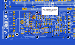
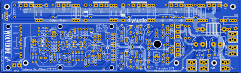
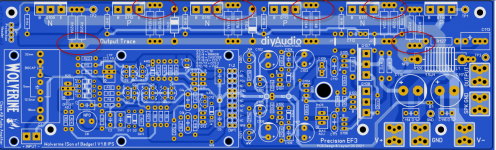
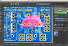
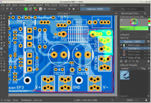
Here is some drawings of the current loops.
First picture is the current loops for the PSU caps and the PSU input. These are the areas where the rectified OPS currents have been physically separated, so they radiate strong even harmonics. At HF the total loop area decreases because the capacitors shunt some of the current.
Second picture shows the feedback current loop. Notice that it entirely overlaps the capacitor current loop. Overlapping loops have 100% coupling. This means that the voltage that appears across the inductance of the capacitor loop will be coupled to the feedback signal at a 1:1 ratio. The areas that don't overlap couple according to the inverse square law and their distance to the offending current loop.
3rd picture shows an alternate feedback route that eliminates almost all the loop area, but will probably require a jumper, and it would help to turn the PSU terminals 90 degrees.
Attachments

What surprises me is that FB ground (G1-G2-G2-G2-Rlift) is also used for other parts of the circuit. Is this not a problem? I would split this into two traces (G1-G2-G2-G2 and G1-Rlift).
Also, C114 and 116 look wrong and should be placed closer to the output devices. Perhaps, swap the place of the power and output on the board.
What other parts of the circuit need to have low inductance?
I tried to work with Sprint to make the changes, just don't have the patience after using Eagle.
- Home
- Amplifiers
- Solid State
- DIYA store "Wolverine" (Son of Badger) .... suggestions ??