


I have a feeling that Nelson Pass put that double pole switch in the circuit design and on the PCB layout, because he felt it was essential. I have a feeling he carefully considered the idea "maybe I could omit the second half of the switch" and after thorough examination, decided he could not.
Yes, you can just short where the 2nd pole goes and use it - it will just
have a larger turn-off thump, but not a turn-on thump. This was simply
the simplest approach.
More sophisticated approach would add two transistors and two more
resistors...


channel module evidently got banged - there is indent in edge of T profile, above VFet
be sure that side going on hsink is flat (no indentation and similar bruises), with prescribed screws there is no torque force to overcome even slightest deformation of surface
not likely the case, but worth saying
be sure that side going on hsink is flat (no indentation and similar bruises), with prescribed screws there is no torque force to overcome even slightest deformation of surface
not likely the case, but worth saying
Although at first glance everything seems to be fine, I'll take your advice into consideration and check the bracket's surface flatness.
Thanks.
Thanks.
I saw the M3 srews for the fastening of the T profile on the heat sink, my decision is to scale up to M5 for a better feeling.

I did this exact same thing on my P version with the FE. Everything felt more natural, no wires crossing from front to back and back to front of the board. Shorter input path. But putting the third screw was really hard, and, after some tests, not needed.…I've reversed the FE board mounting and opted for just two stand-offs rather than loop the various connections…
Looking forward to your pics.
Regards,
Rafa.
that is not error, really
call it Artist's Freedom
or you can call it - another Thinking Trap for Greedy Boyz
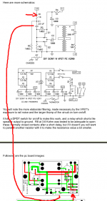
observe - R5 is still outside, to bleed C1
call it Artist's Freedom
or you can call it - another Thinking Trap for Greedy Boyz
observe - R5 is still outside, to bleed C1
Yes, board and schematic do differ. But I think the way it is implemented on the PCB makes more sense - capacitor C1 as first element in the signal path, and R1 being able to function as gate stopper, connected directly to the gates of the JFETs.
Best regards, Claas
Best regards, Claas
Last edited:
- Home
- Amplifiers
- Pass Labs
- DIY Sony VFET pt 2 (N-Channel Build)