Very Flat piece of steel…220 grit….patience. Don’t let your paper clog i.e. clean often. Insure you countersink heatsink holes slightly after. I also use bottoming tap & vacuum.
Oh I see, I'm somewhat familiar with it, just a brain farther on the name. Time to put some of my knife sharpening tools and stones to work.
Very Flat piece of steel…220 grit….patience. Don’t let your paper clog i.e. clean often. Insure you countersink heatsink holes slightly after. I also use bottoming tap & vacuum.
Wet... You can use the water to clear the paper, so get paper that is rated for wet. It's almost impossible to keep fine paper from loading up without going wet. Wet will load as well, what you want to do is quench often, before it starts to load. Wet your work too.. If the work starts to get dry, you need to quench more often. 😉
I'm not talking mist, I'm talking about sanding it in a tank of water... not really, but close.
The finer the grit, the harder to keep it from loading... Alum loads up rapidly.
JT
Last edited:
Wet... You can use the water to clear the paper, so get paper that is rated for wet. It's almost impossible to keep fine paper from loading up without going wet. Wet will load as well, what you want to do is quench often, before it starts to load. Wet your work too.. If the work starts to get dry, you need to quench more often. 😉
I'm not talking mist, I'm talking about sanding it in a tank of water... not really, but close.
The finer the grit, the harder to keep it from loading... Alum loads up rapidly.
JT
I don't think I have the ... to put the precious vfets and other parts near water.
I spray glue (Super 77) sandpaper to glass for lapping. just get some 1/4" thick glass big enough to fit a sheet or two of sandpaper and move the part not the glass. For parts that I really need straight and smooth I step up to much higher than 220 grit. If you have a big enough piece of glass and enough patience you can fix a warped engine head on the ol' lawn mower with this method.
I use a fine grit (red DMTJ diamond whetstone, just to knock down the high spots. Clean and lube with naphtha. Thermal grease takes care of the rest.
I don't think I have the ... to put the precious vfets and other parts near water.
Epoxy packages of semiconductors are watertight. I regularly wash mosfets with soap.
For deburring power transistors I've transitioned from a diamond whetstone to a Japanese "water stone", which I perceive to be less aggressive. Specifically a King KW65, as recommended by many kitchen knife skill instructors on YouTube. (amazon link)
BTW the precious VFETs are in steel TO-3 packages with no epoxy.
BTW the precious VFETs are in steel TO-3 packages with no epoxy.
I too, use stones, and have a toolmakers flat from the old days. (Glass works well too)
My general post was more about sinks than devices.
For devices, I take a more conservative approach, knock down the highs and let the goop deal with any lows. Most of the devices need a very small amount of help, if any. It's more about highs and burrs that might pierce Keratherm, or cause an edge to dig/cut... Ceramic pads are less prone to problems in that area.
NOTE:
Check the (device/s) edges too especially if you are lapping. You can lap something real flat only to create a knife edge that will cut a pad and cause a short. When I’m satisfied, as to the surface, I come back and de-burr the edges.
Again, ceramics are less of a problem.
Just to be clear, are we talking about lapping the bracket, the side that makes contact with the heat sink?
In case anyone else is confused, there is a J108 jfet that is an N channel device. Not to be confused with the 2SJ108 P channel device included in the kit.
Quote: 'Yes & as well the heatsink.'
Surely the whole point of the goop is to make lapping unnecessary? Papa's term 'audio nervosa' springs to mind.
Having said that, my own symptoms require minimal hook-up lengths &/or shielding. I've reversed the FE board mounting and opted for just two stand-offs rather than loop the various connections. Maybe a legacy of playing with RF circuits years ago, but it also seems so much more neat and logical. (The small board is rock solid with just the two screws - no need to drill, tap (and de-burr) two more holes.)
DPST should arrive today, shortly to be followed by first listen. 🙂
__________________
My nervousness started when I saw a 2SK182 go up in temperature, the case) while bolted with the grey heat-mat to the heatsink. Turned out:Quote: 'Yes & as well the heatsink.'
Surely the whole point of the goop is to make lapping unnecessary? Papa's term 'audio nervosa' springs to mind.
- the thermal drift due to not even bottom of the SIT
- might have been the reason for the gate current. 9this was the second device, first one OK + flat)
So my take away was: make sure all contacts where the thermal watts must flow should be pristine. I used a whetting stone bought for the kitchen. Since then it is stable. And I use Wakefield-vette 120 now with mica - not just the sillicone mat. Look at it as a a cylinder head.
I did all that because of having become very very nervous.
Last edited:
In case anyone else is confused, there is a J108 jfet that is an N channel device. Not to be confused with the 2SJ108 P channel device included in the kit.
Thank you
In my kit is also only a single throw switch - but this is easy corrected usually. I wonder why we also could probably omit the second switch and use only the main one? (and/or raise the value of R8 a bit?)
I have a feeling that Nelson Pass put that double pole switch in the circuit design and on the PCB layout, because he felt it was essential. I have a feeling he carefully considered the idea "maybe I could omit the second half of the switch" and after thorough examination, decided he could not.
On the other hand, it certainly is a quick and inexpensive experiment to try yourself. Wire up the amp with a single pole switch and listen to it for a few days. Then wire it up again with a double pole switch instead, and listen to that version for a few days. Is there any audible difference at all? If so, you'd naturally choose the one that sounds best to you. If not, flip a coin.
On the other hand, it certainly is a quick and inexpensive experiment to try yourself. Wire up the amp with a single pole switch and listen to it for a few days. Then wire it up again with a double pole switch instead, and listen to that version for a few days. Is there any audible difference at all? If so, you'd naturally choose the one that sounds best to you. If not, flip a coin.
Hi all,
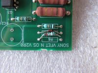
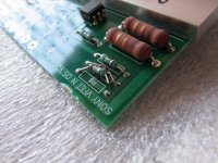
I received my parts kit yesterday. One of the OS shows damage close to R6 and Z2, but none of the packaging (neither exterior nor interior) shows evidence of abuse, on the contrary, they are impeccable. I assume the OS suffered some accident before packaging. But, these are things that happen...
The R6 resistor is broken and the Z2 diode also raises some suspicions, so I decided to replace both components.
According to Mr Pass's article on the "DIY Sony VFET amp pt 2" R6 is a resistance with a tolerance of 1%.
However, given that the OS has been biased by Mr. Pass and I don't know if R6 plays any role in getting the proper bias, I'm not sure if I can simply replace R6 with another resistor with a 1% tolerance, or if I will need to measure R6 and replace it with another resistor with a value closer than 1%?
Can someone enlighten me please?
Thanks.
Attachments

- Home
- Amplifiers
- Pass Labs
- DIY Sony VFET pt 2 (N-Channel Build)