That cap will not have more than a few volts on it. no problem.After the order was placed, I realized that I ordered every component with a 50V voltage rating, except for C12, I somehow have that capacitor at 35V.
Is this a problem now?...the capacitor is "only" on the VIN- pin, the aux signal is not going to reach 35V, right?
The 18v one has 8 amps the 24v has 6 amps. Same power because P = V x I ( the power (P) in an electrical circuit is equal to the voltage (V) multiplied by the current (I). ) . so P = 18V x 8.33A , P = 149.94 , 149.94x 2 = almost 300W , so 300VA transformer.I would kindly ask what the difference is, if the VA rating remains the same at 300VA, but the voltage output changes.
P= 24V x 6.25A = 150W , 150x2 = 300W.
The 2x 18 V transformer is good. Get the 2x 24v only if you want more output power from the amplifier . ( higher voltage rails = higher voltage swing on the amp
You might not need it , because your board has one.Bridge rectifier:
I'll get the first one, ( the one with more caps. ).Rectifier Board:
I changed opinion and now decide that it may be better to buy a finished option, just can't beat those prices.
What I found, since the option given by @xXBrunoXx is not available on amazon anymore.
1)
https://www.amazon.it/Fafeicy-Raddr...da+doppio+raddrizzatore+lm3886,aps,152&sr=8-4
Protection Board:
@xXBrunoXx, do you have any recommendation for that?
I found a few here :
https://www.amazon.it/s?k=speaker+p...eaker+protection+board,aps,119&ref=nb_sb_noss
You can get one and try it.
You might get another small transformer for the speaker protection board, and u can also use it for a relay that turns the big transformer on and off.Except for the speaker components, am I still missing something?
another approach is to get the big transformer with an additional 9 - 12v output, or get some wire and wire yourself one on the ones you mentioned.
( you'll need to wrap a few turns and measure the voltage , so you know how many turns for 9 - 12v.
https://www.conrad.de/de/p/hahn-bv-...tor-1-x-230-v-1-x-9-v-ac-10-0-va-2827696.html
https://www.conrad.de/de/p/hahn-bv-...or-1-x-230-v-1-x-12-v-ac-10-0-va-2827697.html
OR you can get a " power brick" 12v 1A - 2A is enough and you can find them for cheap.
https://www.amazon.it/TEMPO-Aliment...&qid=1734555957&sprefix=12v+2,aps,115&sr=8-12
This would be the easiest and cheapest option for powering the DC protection board and for a relay to turn on off the big transformer.OR you can get a " power brick" 12v 1A - 2A is enough and you can find them for cheap.
https://www.amazon.it/TEMPO-Aliment...&qid=1734555957&sprefix=12v+2,aps,115&sr=8-12
Wait...the easiest and cheaper way to obtain 12-15V is to reduce the voltage from amplifier's (positive) supply. Resistor+zener or regulated by transistor ( an IC for the task is already not cheap and easy...I mean it's about 5€ vs.1€)
A zener won't have enough power for the relays on the DC protection board.Wait...the easiest and cheaper way to obtain 12-15V is to reduce the voltage from amplifier's (positive) supply. Resistor+zener or regulated by transistor ( an IC for the task is already not cheap and easy...I mean it's about 5€ vs.1€)
And 25 - 30V DC is to much for a 12v regulator ( 7812 ) .
I think I am going for the 12V power brick to power the following protection board:
https://www.amazon.it/JINGERL-Indep...efix=speaker+protection+board,aps,119&sr=8-30
This is the relay I would pick, the images show a 10A switching power so I guess it would be enough right?
https://www.amazon.it/GTIWUNG-Fotoa...=1734859124&sprefix=relay,aps,137&sr=8-7&th=1
This may sound stupid, but why do I need a separate way to switch the transformer on and off?
@xXBrunoXx
Again a question to the layout of the PCB, didn't you post a link to the layout guidelines for the PCB?...I can't find it anymore...
That relay board looks good, you get 10 boards for 13 euro.This is the relay I would pick, the images show a 10A switching power so I guess it would be enough right?
https://www.amazon.it/GTIWUNG-Fotoa...=1734859124&sprefix=relay,aps,137&sr=8-7&th=1
This may sound stupid, but why do I need a separate way to switch the transformer on and off?
You don't need it but it's good practice to use a relay instead of a tiny switch.
Reliability and it's "more safe " to have 12v on the switch not 220.
First page post #8Again a question to the layout of the PCB, didn't you post a link to the layout guidelines for the PCB?...I can't find it anymore...
https://neurochrome.com/pages/stability
That board is mono , you need 2 of them. Also they seem to be out of stock.I think I am going for the 12V power brick to power the following protection board:
https://www.amazon.it/JINGERL-Indep...efix=speaker+protection+board,aps,119&sr=8-30
Thank you again, completely overlooked it...First page post #8
And completely missed that too....That board is mono , you need 2 of them. Also they seem to be out of stock.
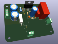
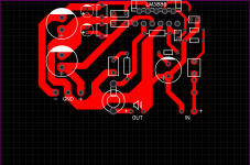
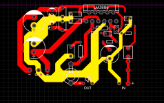
Allright, this is waht I managed to do with the layout...
It is a 2 layer board, GND on bottom and all the rest on top
I decided to go with filling zones for the V- and V+ input line, because the component layout allowed for it, but I do not know if this is a good idea...
The rest of the connections are 5mm traces, I tried to keep them as far apart and to avoid having them in parallel.
From what I understand, reading the recommended article and further online articles, the feedback loop has to be as close as possible to the output of the amplifier, so I placed R8 and C12 as they are.
Same with the zobel network, R4 and C10.
For the heatsink support, I thought about leaving some extra space behind the amplifier, so it can rest on the PCB, as alternative for the mounting brackets.
In general I tried to keep the components as close as possible to the amplifier.
This of course is just my layout, I have never done a layout for an amplifier circuit and therefore am open to any suggestions.
Attachments
Hi, I was wondering what you've been up to , with the amp, I did not get a notification on your last post . Sorry for late reply.
also, Happy new year !.
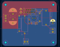
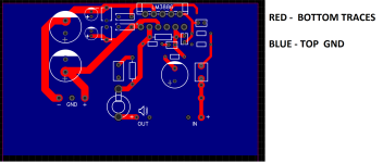
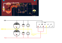
- Your capacitors are wired wrong from what I can see., one terminal to + one to - , and the other remaining + and - terminals are tied togheter to GND.
Re-arrange them.
- Resistor from pin 3 to pin 9 should be close to the ic .
- For easier soldering of the LM3886 I recommend having the traces on the bottom side , TOP side GND , and not having to solder the ic on both sides of the PCB.
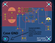
!!!! Having the V- on the PCB holes , will connect them to the case ( amplifier enclosure ) !!!! you will short the V- to case ( amplifier enclosure ) GND !!!. . Usually you have GND on the PCB holes. The case of the LM is connected to V- , ( normally ic's would have GND on the case and heatsink. ) DO NOT Connect the top holes with copper fill . Isolate the heatsink from the amplifier case ( amplifier enclosure ) . or use mica to insulate the LM's from the heatsink. For better thermal connect the LM's dirrectly to the heatsink and insolate the heatsink from the Amplifier case. from the 4 holes on the PCB , only connect one with copper fill to GND, and connect it trough the screw on the case , make there the connection with the transformer / power supply rectification board GND . Leave the other 3 holes with no copper on them. !!!
also, Happy new year !.
- Your capacitors are wired wrong from what I can see., one terminal to + one to - , and the other remaining + and - terminals are tied togheter to GND.
Re-arrange them.
- Resistor from pin 3 to pin 9 should be close to the ic .
- For easier soldering of the LM3886 I recommend having the traces on the bottom side , TOP side GND , and not having to solder the ic on both sides of the PCB.
!!!! Having the V- on the PCB holes , will connect them to the case ( amplifier enclosure ) !!!! you will short the V- to case ( amplifier enclosure ) GND !!!. . Usually you have GND on the PCB holes. The case of the LM is connected to V- , ( normally ic's would have GND on the case and heatsink. ) DO NOT Connect the top holes with copper fill . Isolate the heatsink from the amplifier case ( amplifier enclosure ) . or use mica to insulate the LM's from the heatsink. For better thermal connect the LM's dirrectly to the heatsink and insolate the heatsink from the Amplifier case. from the 4 holes on the PCB , only connect one with copper fill to GND, and connect it trough the screw on the case , make there the connection with the transformer / power supply rectification board GND . Leave the other 3 holes with no copper on them. !!!
Attachments

Hello again, happy new year!
- If I understand it right, you mean the filter capacitors for the input voltage of the IC, going from C1 to C7, right?
If I compare them with the schematic you mentioned here:
- Okay, moved the resistor closer to the IC, are there any other components with priority that should be connected as near as possible to the IC?
- So I guess I have to do the whole layout again, what trace width are you using/recommend using?
The 4 holes on the PCB are mounting holes in Kicad, they have a extra symbol for it and are not connected to anything (or at least on the other PCB I made, a Buck converter, it was like this).
What I planned to do is to use a transparent plexiglas enclosure and keep everything in sight. But from the adapted picture you made, I guess I need to have one hole connected with the GND plane to be able to connect the PCB GND to the supplyboard?
Thank you again.
- If I understand it right, you mean the filter capacitors for the input voltage of the IC, going from C1 to C7, right?
If I compare them with the schematic you mentioned here:
They should be connected the same way, or am I missing something?No problem with that.
- Okay, moved the resistor closer to the IC, are there any other components with priority that should be connected as near as possible to the IC?
- So I guess I have to do the whole layout again, what trace width are you using/recommend using?
The 4 holes on the PCB are mounting holes in Kicad, they have a extra symbol for it and are not connected to anything (or at least on the other PCB I made, a Buck converter, it was like this).
What I planned to do is to use a transparent plexiglas enclosure and keep everything in sight. But from the adapted picture you made, I guess I need to have one hole connected with the GND plane to be able to connect the PCB GND to the supplyboard?
Thank you again.
Using plexiglass enclosure won't matter then. So your ground plane on the pcb connected to a 3 pin header, with the + and - is fine. it connects to the power supply board. No need to connect wires to / trough the holes , screws.The 4 holes on the PCB are mounting holes in Kicad, they have a extra symbol for it and are not connected to anything (or at least on the other PCB I made, a Buck converter, it was like this).
What I planned to do is to use a transparent plexiglas enclosure and keep everything in sight. But from the adapted picture you made, I guess I need to have one hole connected with the GND plane to be able to connect the PCB GND to the supplyboard?
The supply caps should be close enough to the ic.are there any other components with priority that should be connected as near as possible to the IC
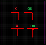
for signal won't matter that much how thick the traces are , avoid 90 degree bends.what trace width are you using/recommend using?
For the + and - you can make them thicker , as much as you want, if you have space . on my pcb they are 3 or 4 mm. For the speaker output I used 2mm. even 0.2mm would be sufficent, because the traces are short, but if you have the space , why not make them thicker.
I have 1 mm traces for signal. You have the space make them thick, Filling the traces like you did for + and - is good .
Attachments
Thank you for your detailed response!
However, I'm still a bit confused about which specific capacitors you meant that I may have connected incorrectly.
I've gone through the circuit again but can't seem to pinpoint them.
Could you explain to me again which capacitors you meant? Sorry if this may sound stupid, but I can't seem to find them.
Hello,
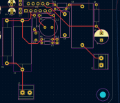
@xXBrunoXx I updated the schematic and PCB as you suggested, you drew a separate GND trace in the pictures, is the top GND plane enough or do I need a separate GND trace for the input capacitors?
Because from the past pictures you posted about your design, you made a separate trace, but the GND traces are all connected together, right?
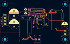
@fancy_user_123 All GND's are connected to the ground plane.
I made two versions, one with ground plane and one star ground ( almost ).
Yellow is one trace practically , GND.
I made two versions, one with ground plane and one star ground ( almost ).
Yellow is one trace practically , GND.
Attachments
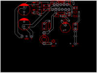
Allright, 2nd attempt
I switched the top and bottom plane, now GND is on top and the rest on bottom.
I made the traces thicker, up to 2mm.
I switched the position of R6, so that it is near to the IC.
I made zones again, where the space allowed it.
I switched the top and bottom plane, now GND is on top and the rest on bottom.
I made the traces thicker, up to 2mm.
I switched the position of R6, so that it is near to the IC.
I made zones again, where the space allowed it.
Attachments

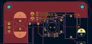
Allright, changed that too. If there isn't anything else, I guess I can order the components and give the PCB to jlcpcb.GND and V+ are shorted from what I see.
As soon as I have everything together, I am going to post the result here 🙂
Thank you again for the patience and help I got from the community.
- Home
- Design & Build
- Electronic Design
- DIY PC/Desktop Setup