
Any chance of a Wolverine Meetup in the reasonable future?...Would love to meet some of you geeks and have a beer or 2 while sharing our Wolverine experience. In the youngtimer car scene this is more or less a regular thing but I guess the international nature accompanied with huge distances and some of us even living down under for crying out loud 😊... prevents this from coming alive🙂....
w.
w.
Dan,
For absolute beginners like myself your video's are an invaluable resource.
Thank you very much.
Richard
For absolute beginners like myself your video's are an invaluable resource.
Thank you very much.
Richard
^ Agreed. The effort taken to share expert-level knowledge and present it in a way for a novice, like me, to have confidence in achieving a successful build is appreciated far more than can be understood.
I hope, one day, to comprehend a great deal that goes into these designs. For the moment, I am studying, and am but a humble 'assembler of parts'.
The attention to explaining, why, and providing examples of commercial products for considerations and inspirations stand out to me as exemplary additions to a sensational video series. Kudos.
@danieljw - Thank you!
Speaker cable bridge as per Daniels instruction video. Might add some cable sleeving...not sure yet.

Wow what a wonderful job you've done. Awesome work.Speaker cable bridge
zip tie mounts
Get yourself some cable clamps and you'll be able to fully tidy up your wiring.
The ones with a 3mm hole are the ones I generally use.
Last edited:
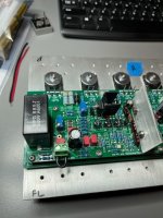
I have reached the end of my trouble-shooting knowledge, so I'm hoping all the experts here can help me out.
Built (2) GB1 boards, labelled "A" and "B" - B board works, set the CCS to 5V, bias at 40mV and offset to 0. Started first on a DBT and then after 10-15 mins. went full voltage and everything worked great.
Board "A" not so much - it is cycling/surging the DBT (glows bright, then dims a little and repeats). Can't set the CCS (shows ~2.5V), can't set the bias, as it fluctuates from 100mV up to 300mV, cycling up and down with the DBT glowing brighter, cycling. looked at offset and it's at ~1.25V. My PSU is 65V, with the DBT on the working channel it is ~55V, but board "A" the voltage is drawing down to ~10V - assume a large short of some kind or switched transistors, but I can't find it.
What troubleshooting I have done so far:
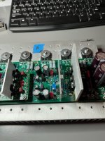
1) compared every part to the working board to make sure all resistors, diodes, transistors and trimmers are correct for value and orientation
2) Checked all transistors for BCE junction with the DMM - they all appear to be good.
3) drawing down my PSU voltage from 65Vdc to ~10Vdc, assume there was a short (big). I cannot find anything shorting to ground or the heatsink (tested with one probe on the speaker ground, PSU ground and heatsink (all heatsinks) while going over every components solder joint with other probe, waiting for a "beep", there was none
4) took board off the heatsink and checked both the front-end and output boards for any bad solder joints. Thought I saw a few questionable ones on the 14-pin connector, so I resoldered each of those. along with 4-5 other ones that didn't look perfect.
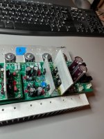
Put it all back together and tried to power-up again, and same thing. DBT lights and cycles bright and brighter, the LEDs on the board light and basically "blink" as the DBT and bias cycles, up and down.
I would take some measurements, but I don't want to leave it running like this, even with a DBT.
Any ideas where to look (again), I really thought I just switched a diode or a transistor, but I have confirmed it is exactly the same as Board "B".
Transistors chosen, all checked and matched with B&K tester, multi-tester, or both before installing:
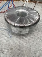
PSU - currently testing with +/-65Vdc and 40k uF filtering
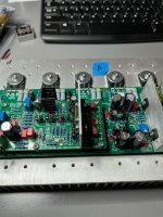
Built (2) GB1 boards, labelled "A" and "B" - B board works, set the CCS to 5V, bias at 40mV and offset to 0. Started first on a DBT and then after 10-15 mins. went full voltage and everything worked great.
Board "A" not so much - it is cycling/surging the DBT (glows bright, then dims a little and repeats). Can't set the CCS (shows ~2.5V), can't set the bias, as it fluctuates from 100mV up to 300mV, cycling up and down with the DBT glowing brighter, cycling. looked at offset and it's at ~1.25V. My PSU is 65V, with the DBT on the working channel it is ~55V, but board "A" the voltage is drawing down to ~10V - assume a large short of some kind or switched transistors, but I can't find it.
What troubleshooting I have done so far:
1) compared every part to the working board to make sure all resistors, diodes, transistors and trimmers are correct for value and orientation
2) Checked all transistors for BCE junction with the DMM - they all appear to be good.
3) drawing down my PSU voltage from 65Vdc to ~10Vdc, assume there was a short (big). I cannot find anything shorting to ground or the heatsink (tested with one probe on the speaker ground, PSU ground and heatsink (all heatsinks) while going over every components solder joint with other probe, waiting for a "beep", there was none
4) took board off the heatsink and checked both the front-end and output boards for any bad solder joints. Thought I saw a few questionable ones on the 14-pin connector, so I resoldered each of those. along with 4-5 other ones that didn't look perfect.
Put it all back together and tried to power-up again, and same thing. DBT lights and cycles bright and brighter, the LEDs on the board light and basically "blink" as the DBT and bias cycles, up and down.
I would take some measurements, but I don't want to leave it running like this, even with a DBT.
Any ideas where to look (again), I really thought I just switched a diode or a transistor, but I have confirmed it is exactly the same as Board "B".
Transistors chosen, all checked and matched with B&K tester, multi-tester, or both before installing:
- KSA992, C1845
- BC550 (B), BC560 (B)
- A1381 (E), C3503 (E)
- Q103/Q104 are both BD13916S
- Drivers - A1837, C4793
- Outputs - MJL4281 and MJL4302A
PSU - currently testing with +/-65Vdc and 40k uF filtering
Attachments
Hi Bullittstang,
Have you removed the jumper link that is used during the steps in the build guide ?
Failing that being the problem you can remove the input stage board and test it in isolation and to rule any problems out and then go through the checks in the build guide
Also you can look at both boards side by side and see if there is a difference somewhere
- hope this is helpful, let us know how you go
Thirded! This is an amazingly helpful video for any amp builder. Just wow.
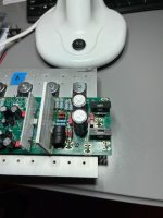
Its hard to say as your photos aren't that clear.Board "A" not so much - it is cycling/surging the DBT (glows bright, then dims a little and repeats). Can't set the CCS (shows ~2.5V), can't set the bias, as it fluctuates from 100mV up to 300mV, cycling up and down with the DBT glowing brighter, cycling. looked at offset and it's at ~1.25V. My PSU is 65V, with the DBT on the working channel it is ~55V, but board "A" the voltage is drawing down to ~10V - assume a large short of some kind or switched transistors, but I can't find it.
It sound like you have a short or a component installed incorrectly.
Its also possible is a damaged component.
Generally if the output bias is set to maximum resistance on the R109 pot.
Then with the input shorted you should reach full rail voltage.
If you don't there is no point adjusting anything. You have a problem.
This test only need be preformed for a few seconds.
So I noticed that you have top adjustable timpots so for R109 maximum resistance will be when R109 it turned fully clockwise.
I have a few Questions.
1. Did you follow the build guide for the entire start up procedure ?
2. Did you test the both the ips and ef3 board together with no outputs installed ?
If yes, then please check you have removed jumper J103 (But I'm assuming you know that as you have one board working)
Please check your outputs are definitely in the correct position.
If no, Please remove your outputs and preform the tests in the build guide.
3. If its still not working go to the trouble shooting section in the build guide and test each board individuallyFeel free to check my build album for a few more images on how to do this.
Good luck
Unless you want internal electrical field shieldings, you could add one externally to short stray magnetic field, can't you.
Thanks Daniel and Stuart.Hi Bullittstang,
Have you removed the jumper link that is used during the steps in the build guide ?
Failing that being the problem you can remove the input stage board and test it in isolation and to rule any problems out and then go through the checks in the build guide
Also you can look at both boards side by side and see if there is a difference somewhere
- hope this is helpful, let us know how you go
1) I didn't follow the start-up procedure without the outputs, but might go backwards and try that if I can't figure it out.
2) testing the IPS in isolation - am I correct with this wiring
- G1/G2 both connected to PSU 0V
- NFB, ND- and PD+ are all shorted together - is there a wire run from these three points back to "between cathode D5 and Anode D6"??
- V+ and V- connected to PSU +, - (this is pretty clear)
Want to mainly confirm that no other bridges or connections are needed to test. (See NFBND-/PD+ question above)
Here is a picture, which might make it clearer for testing the input stage

Daniel - you are the BEST!!!! A picture is certainly worth a 1000 words (or more)
Also good news - front-end is working perfect, can easily set the CCS to 5V (5mA) and nothing heats up and the offset is <10mV.
On to the output board - I already confirmed the outputs are correct and in the right spot PNP to NPN on the board. So back out with the Board "B" and the magnifying glass to figure out where I have a short coming from
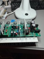
BOTH CHANNELS ARE WORKING - thanks for all the help and ideas to track it down guys. Came down to a very dumb oversight - I will blame it on a late night assembly, but really no excuse - flat out brain-fart.
ISSUE - Q104 (VBE) was flipped around, had the front of the transistor screwed to the heatsink, which of course makes the pinout backwards on the board.
How I found the issue - since I couldn't see Q104 even with the board removed from the heatsink (covered in thermal paste). I tested the diode drop from the Cathode of D106A to ECB of Q104. the voltage drop from cathode to ECB was higher than the other channel, 0.653 vs. 0.409 on good channel. So I first pulled out D106A to make sure I had a BAV20/21 installed. I did, so then I pulled out Q104 thinking it was bad or got shorted at power-up. At this time I'm not remotely thinking it was filled around, since I still had thermal paste and when I tested the leads the DMM tol me it was bad. Always wanting a confirmation, since it's a brand new part from Mouser, I stuck in the multi-tester and tested good, WHAT??? Then I cleaned it off and found the lettering on the heatsink side and leads bent the wrong way.
Luckily I powered it up with a 60W bulb in the DBT. My mantra has been and will always be... first power up with the DBT. Saved my butt today and countless other times after an assembly or repair (that I thought was correct).
Great guide @danieljw , @stuartmp and @fireanimal and to the countless other people contributing to this project, you guys truly did an amazing job on the board, the testing, the guide, the pictures and the ongoing help for guys like me to find problems.
Now that I know they both channel work I am re-motivated to get the chassis/PSU completed and listen to some music!
@bullittstang given you are using the new bias transistors, Q104 is no longer mounted to the heat sink. Q103 is on the main heat sink with fly wires in an EF3-3.
- Home
- Amplifiers
- Solid State
- DIY Class A/B Amp The "Wolverine" build thread