What I was doing was biasing a bank of power Darlingtons so their large currents tracked temperature and were also shared equally. It's essentially the same problem whether single or multiple devices are conducting microAmps (like a bandgap regulator) or kiloAmps (like a large power supply).Nice application but we are talking biasing here.
You are talking current equalizing , a very different use.
As a side note, you are talking 20A current levels, OP is talking milliamps.
Last edited:
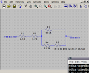
Before I order the parts I am checking what real values are available. As the Base-Emitter resistor of the VBE multiplier cannot be a preferred value, I had to use rather complicated workarounds to get what simulations are strongly indicating. The indicated value is 580 Ohms, but variations of only 5 Ohms in this resistance result in quiescent currents of 40mA per pair, which means, the variable resistor has to be accurate and low and must allow me to reliably change the resistance by a fraction of an Ohm and keep that value. Since, this requirement is quite rigid and the lowest potentiometer value is 100 Ohms, I used a resistor network of several resistors and a pot of 100 Ohm to give a resistance variability of 15 Ohms. The latter provides more than enough range to set the bias correctly, at least, simulations corroborate that.
Attachments
Ed, as a sanity check, look at a couple of representative amplifiers.
Are there any with such a convoluted network? What would that tell you?
Jan
Are there any with such a convoluted network? What would that tell you?
Jan
jan.didden said:Are there any with such a convoluted network? What would that tell you?
This project could not start from a tabula rasa, but I had to start basing on already existing circuitry. The original was a Wharfedale 1500S PA amplifier which failed. Due to most of the original circuitry being implemented in SMD, and due to the fact that it used a grounding scheme where the hot output point was ground and the usual 0V point the output, I revamped the circuit altogether and kept the output stage, driver stage and the power supply. The rest was removed and the ground re-implemented to use the 0V point as ground. As if this was not enough, the output stage is implemented in CFP configuration. The latter, is known to be extremely sensitive to bias changes, hence the stringent requirement of having a setting necessitating very small and reliable resistance changes. This amplifier, after the drastic lobotomies, already gave me a service of two years and I liked the sound. So, I am ready to bend backwards to have it repaired and use it.
This is exactly what I do. I use a BC847C as the sense transistor and an 857C as the pass transistor. The drivers and pre drivers share the same heatsink as the output devices. I couple the BC847C to the collector leg of one of the centrally mounted output devices with some thermal grease. On some layouts, the compensation was too much and Iq went down. I fixed this my removing the thermal grease. I get about 10-20% change in Iq from c. 20C to 55C as measured on the heatsink with an IR thermometer.Dear edbarx,
The VBE multiplier is the simplest way to get the required Voltage. Remember, when you multiply the VBE with a multiplier, you also multiply the base-emitter's negative tempco (miiliVolts per degree C ). Using several series-connected diodes from differing technologies may also give you a different tempco. If I recall, a Schottky, like a BAT-54, has a different negative tempco than a Silicon signal diode, like a 1N914.
Ideally, if the VBE multiplier is directly driving a bank of several NPN/PNP output devices, you'd prefer the VBE multiplier's tempco match the output bank's' 2 tempcos. If you use series connected diodes and pad up the forward voltage with a small series resistor, you decrease the effective tempco. Imagine using a large padding resistor, like hundreds of Ohms - you virtually eliminate the desired negative tempco, since most common resistors have tempcos many times lower than forward-biased diodes.
Rather than trying to match thermal time constants by bolting two heat sinks together, I'd use a VBE multiplier with something tiny, with a short thermal time constant like a MMBT2222. and bond it to the heat sink of one the power devices it's driving, using thermal epoxy. Better yet, use JB Weld. It has excellent thermal characteristics and it's available almost everywhere. While steel-filled JB Weld is a poor electrical conductor, I'd stay away from the MMBT's leads with the JB Weld.
What you're doing with the tiny device bonded to the power device, is creating an overall thermal time constant that's ~ that of the power device. While the thermal time constant of the power device is, say, 10 seconds, you've bonded a device to it with a fractional-second thermal time constant, so it tracks very well.
I dont think DS or RC explored this option enough IMV so we’ve ended up with all sorts of beasties to solve what should be a simple problem. Mounting drivers and pre-drivers on separate heatsink also complicates the issue - again only my view.
(BTW I’ve never had a Vbe multiplier failure - seems it’s quite a rugged circuit function).
https://hifisonix.com/audio-amplifier-temperature-compensation/
Where did you read that? 'Somewhere' on the 'net? The majority of power amps use some form of a CFP in the outputs. There's nothing special about the Vbe sensitivity. Read, for example, Bob Cordell (pg 97 ff).the output stage is implemented in CFP configuration. The latter, is known to be extremely sensitive to bias changes,
Or, another well-know author, Douglas Self says in Audio Power Amplifier Design (6th Ed.), pg 237 ff: 'The CFP stage is generally considered to show better thermal stability than the EF because the Vbe of the output devices is inside the local NFB loop, and only the driver Vbe has a major effect on the quiescent conditions" There's more detail to it of course, but that's the gist of it.
You're free to follow any path you like of course, but you may be spending effort where it is misdirected.
Jan

I don't know, the more I learn the more I realise how little I know! I am literally yearning to have that amplifier repaired and working. It is such a pity to leave it on the workbench waiting in vain for its turn. 🙁
It is my experience when I set the bias for the first time for this amplifier that I found it was so difficult that I had to try different resistor values. However, I did not find a decent quality pot, but a cheap carbon type one with a value of 220 Ohms. The quiescent current control was abrupt, at first no current at all, then it increased very rapidly, and finally it ran into amperes.
I want a decent quiescent current control which starts from zero current to about 20mA per pair when the pot is turned fully. The contortion I humbly devised should provide me with such a control. Yes, I admit to all and myself included: it is not elegant, it is not attractive, it is very uncommon, but it should provide what I need.
The pot on a Vbe multiplier should be wired to fail safe. That is go high resistance and turn output to zero volts on failure.The likely hood of a bjt used as a Vbe multiplier for failure is very low. It usually passes the VAS current which is not much more than ~10mA. In many cases the device selected is a power bjt such as a BD139 so even less likely to fail so I think your concerns are unrealistic. If anything is to fail it might be the pot.
The problem with diodes is you get 0v7 1v4 2v1 so the steps are too big to be accurate enough.
The reason for using a network of resistors to achieve a resistance range of a few tens of Ohms is I could not find potentionmeters of the right size. I needed a pot of 15 Ohms with the original calculations but I found potentiometers of 10R, 100R, 200R, ... , 1k, 2k, ... A simple network of resistors can be used to shrink a pot's range and yet allow a user to use its entire rotational variability. This gives much more definition per radian/degree. With a simple setup the definition can be increase by a factor of six. This allows better manual control of the bias or whatever purpose it is used for.
Let us consider two resistors Ra and Rb to be in parallel. Their equivalent resistance is given by:
Now, let us assume Rb to be composed of two series resistances, x and y.
Rb = x + y
Substituting in (b):
Differentiating with respect to y, the pot setting:
As an example consider two 1k resistors and a 100R pot connected as explained above.
The linearity of total resistance change while changing x, depends on the gradient remaining practically constant.
When the pot is set at 0R:
(i.e. the equivalent resistance changes by only 0.25 Ohms per unit (1 Ohm) change in th pot. This is a magnification of 4).
When the pot is set at 100R:
(i.e. the equivalent resistances changes a little less per unit but still the value is almost the same as the first one).
Let us consider two resistors Ra and Rb to be in parallel. Their equivalent resistance is given by:
Code:
1/R = 1/Ra + 1/Rb ....... (a)
=> 1/R = (Rb + Ra)/(Ra*Rb)
=> R = Ra*Rb/(Rb + Ra) ...... (b)
Now, let us assume Rb to be composed of two series resistances, x and y.
Rb = x + y
Substituting in (b):
Code:
R = Ra*(x + y)/(x + y + Ra) ...... (c)Differentiating with respect to y, the pot setting:
Code:
dR/dy = {(x + y + Ra)Ra - Ra(x + y)*1}/{(x + y + Ra)^2}As an example consider two 1k resistors and a 100R pot connected as explained above.
The linearity of total resistance change while changing x, depends on the gradient remaining practically constant.
When the pot is set at 0R:
Code:
dR/dy = {(1000 + 0 + 1000)1000 - 1000(1000 + 0)}/{(1000 + 0 + 1000)^2}
dR/dy = 0.25 OhmsWhen the pot is set at 100R:
Code:
dR/dy = {(1000 + 100 + 1000)1000 - 1000(1000 + 100)}/{1000 + 100 + 1000)^2}
dR/dy = 0.227 Ohms
Last edited by a moderator:
Modelling a potentiometer's characteristic to behave similar to the mathematical inverse of a BJT's input characteristic.
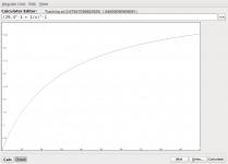
This post will discuss how to obtain a resistance characteristic* with a logarithmic-like shape. The characteristic has a horizontal asymptote, which means, the effective resistance value cannot exceed a certain predetermined value.
Consider two parallel resistors A and B. The effective resistance is given by:
1/R = 1/A + 1/B ........ (a)
=> 1/R = (B + A)/(A.B)
Putting R subject, we get:
R = A.B/(B + A) ........ (b)
Now, let us evaluate the limit as A approaches infinity:
Consider B + A as A approaches infinity:
B is insignificant compared with infinity, therefore, B + A ---> A. This implies, in A.B/(B + A), A and (B + A) cancel, leaving only B. Graphically, this means, the combined resistance does not exceed the value of B, and that the gradient will gradually approach 0, a horizontal line.
This property of two parallel resistors can be used to compensate for a BJT's input characteristic ever-increasing steepness to achieve a better manual resistance control while biasing an amplifier. The steep part of the characteristic can be placed in a way, so that, it is effective when the amplifier is underbiased or with no quiescent current at all. As the correct bias is approached, the gradient decreases giving more definition per degree/radian. When the bias is reached, subsequent increases are more difficult to achieve, as they require more resistance which becomes more difficult to increase with small changes of the potentiometer's slider position.
The attached graph illustrates the effective resistance of a 100R potentiometer in parallel with a 29.4R resistor. As discussed above, the gradient is at first steep, then it becomes less and less steep.
* The independent variable is the Pot's set value and the dependent variable is the value of the combined resistance.
Attachments
I haven't tried the math, but it seems two 1% series-or-paralleled resistors would meet the accuracy requirements for any simple NPN/PNP output stage (one without pre-drivers).Modelling a potentiometer's characteristic to behave similar to the mathematical inverse of a BJT's input characteristic.
This post will discuss how to obtain a resistance characteristic* with a logarithmic-like shape. The characteristic has a horizontal asymptote, which means, the effective resistance value cannot exceed a certain predetermined value.
Consider two parallel resistors A and B. The effective resistance is given by:
1/R = 1/A + 1/B ........ (a)
=> 1/R = (B + A)/(A.B)
Putting R subject, we get:
R = A.B/(B + A) ........ (b)
Now, let us evaluate the limit as A approaches infinity:
Consider B + A as A approaches infinity:
B is insignificant compared with infinity, therefore, B + A ---> A. This implies, in A.B/(B + A), A and (B + A) cancel, leaving only B. Graphically, this means, the combined resistance does not exceed the value of B, and that the gradient will gradually approach 0, a horizontal line.
This property of two parallel resistors can be used to compensate for a BJT's input characteristic ever-increasing steepness to achieve a better manual resistance control while biasing an amplifier. The steep part of the characteristic can be placed in a way, so that, it is effective when the amplifier is underbiased or with no quiescent current at all. As the correct bias is approached, the gradient decreases giving more definition per degree/radian. When the bias is reached, subsequent increases are more difficult to achieve, as they require more resistance which becomes more difficult to increase with small changes of the potentiometer's slider position.
The attached graph illustrates the effective resistance of a 100R potentiometer in parallel with a 29.4R resistor. As discussed above, the gradient is at first steep, then it becomes less and less steep.
* The independent variable is the Pot's set value and the dependent variable is the value of the combined resistance.
Ignoring any Beta effects, any Base or Emitter resistors in series with the output devices or any bulk Base or Emitter resistivity inside those same devices, what you're doing with a multiplier is creating a 2 VBE current mirror bias to drive the output stage's 2 VBEs. When the VBE multiplier is set to 2 VBEs, the combined Base Current of the output devices, to first order, should match the Current driving the VBE multiplier transistor.
When the multiplier is set to 2 VBEs, the 2 diode negative Voltage tempco of the multiplier should also match the summed 2 diode negative tempcos of the output's 2 VBEs. The first order bias point shouldn't change significantly with temperature.
Remember, padding up a diode's voltage with series resistance causes it depart from a log characteristic. It also decreases the effective negative Voltage tempco.
Also, remember the forward Voltage of a series resistor & diode as a function of forward Current is entirely predictable with math, while the forward Current as a function of applied Voltage is transcendental and can only be solved graphically or by a series expansion approximation or Newton's Method, except if you're familiar with the Lambert W Function, which still evades me.
Considering a tweak pot, have you looked at log pots, i.e. old fashioned volume controls, to spread out the one-ended crowding? If you don't like carbon pots, a wirewound log pot may work. If you don't like lumpy wirewound pots, they also make logarithmic pots with the wire spiral embedded in Cermet. May not be cheap and may not come in multi-turn trimpots.
Making the VBE multiplier's dynamic performance track the output devices - generally the VBE multiplier is a tiny device whose thermal time constant is much faster than the output device(s). Consider bonding the multiplier to one of the output device's thermal tabs with thermal epoxy or better yet, with common, inexpensive steel-filled JB Weld epoxy, which has excellent thermal conductivity. Just stay away from the VBE multiplier's leads or its biasing resistors with JB Weld.
The bonded VBE multiplier will track the dynamic VBE of that output device within a few seconds - well enough to minimize chances of thermal runaway.
Last edited:
I would like to explain how I am trying to make the VBE multiplier compensate for temperature changes to keep the bias stable.
The VBE multiplier amplification factor was increased to multiply the -2mV/K Vbe drop by a larger factor to compensate for the drivers VBE changes and the output devices VBE changes. This implies a multiplication factor of around 4 is required. The two signal diodes in the driver base path will not be thermally coupled, so that, not to increase the multipling factor beyond 4. Simulations are showing coupling the VBE multiplier transistor, a BD135 NPN transistor, to an output device, 2SC5200 or 2SA1943, should provide temperature compensation and a stable bias current. If more stability is found to be required when the circuitry changes are implemented and the amplifier is tested, a thermistor in series with a sufficiently high resistance should provide the required voltage drop across the VBE multiplier emitter and base. Simulations are strongly suggesting this will not be needed.
I think, I should also mention that the VBE multiplier setting potentiometer is moved from the Emitter-Base junction to the Base-Collector junction and a 42.2 Ohm resistance is added in parallel with the pot to transform the pot linear characteristic into a quasi-logarithmic one.
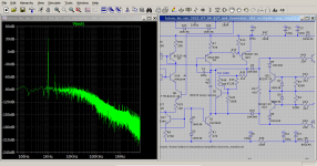
I am posting the LTSpice schematic and screenshots of the Fourier Analysis. The working frequency is 1000Hz.
The VBE multiplier amplification factor was increased to multiply the -2mV/K Vbe drop by a larger factor to compensate for the drivers VBE changes and the output devices VBE changes. This implies a multiplication factor of around 4 is required. The two signal diodes in the driver base path will not be thermally coupled, so that, not to increase the multipling factor beyond 4. Simulations are showing coupling the VBE multiplier transistor, a BD135 NPN transistor, to an output device, 2SC5200 or 2SA1943, should provide temperature compensation and a stable bias current. If more stability is found to be required when the circuitry changes are implemented and the amplifier is tested, a thermistor in series with a sufficiently high resistance should provide the required voltage drop across the VBE multiplier emitter and base. Simulations are strongly suggesting this will not be needed.
I think, I should also mention that the VBE multiplier setting potentiometer is moved from the Emitter-Base junction to the Base-Collector junction and a 42.2 Ohm resistance is added in parallel with the pot to transform the pot linear characteristic into a quasi-logarithmic one.
I am posting the LTSpice schematic and screenshots of the Fourier Analysis. The working frequency is 1000Hz.
Attachments
Last edited:
The idea of using some sort of thermally conductive glue for the transistor is worthy of more explanation as I have never used such a product before. I live in Malta (a very small EU member state). The country is geographically located about 60 miles south of Sicily (Italy).
I stated where I live because I have never seen such a product. In fact, I always use bolts and nuts to fasten transistors to heatsinks.
I stated where I live because I have never seen such a product. In fact, I always use bolts and nuts to fasten transistors to heatsinks.
The parts have been ordered yesterday, but owing to my location and the seller's on the globe, it will take some weeks to arrive. I will prepare the actual physical amplifier modules (see my avatar) for the major surgery: it will improve the distortion figure and it will also improve the bias stability.
Long Life for this amplifier which already gave me a service of two years of beautiful music, and this is thanks to this forum, without which my knowledge of amplifier design would have been complete guesswork.
Long Life for this amplifier which already gave me a service of two years of beautiful music, and this is thanks to this forum, without which my knowledge of amplifier design would have been complete guesswork.
Dear edbarx,
I'd forgotten your location. It sounds like you have a good handle on the Vbe multiplier issues and the large Voltage steps of discrete series diode combinations. My first DIY Class AB crossover bias issue was a 1970, 250 Watt all-NPN home audio amplifier. 7 years later, I turned the design into a 2.5 kiloWatt servo amp to drive a rotating CT scanner gantry. My employer sold ~ 200 of those CTs for $1.2 Million (US) each.
I recently revived a 1961 DIY two transistor regenerative reflex AM/SW receiver and improved its sensitivity 50 times, using LTSpice. The self-bias circuit for those very same two transistors was a toss-up between a Vbe multiplier and a Bob Widlar bandgap regulator.
Now I'm trying to figure out how to reduce Class D crossover distortion by a similar technique, but in the time domain, not the Voltage domain.
My Best,
Ron
Last edited:
The problem with diodes is getting right bias current.
With a Vbe multiplier you can get it spot on.
Too little current gives crossover distortion.
Too much current wastes power as heat.
So long as pot is in BE half of multiplier the pot failing will result in too little current rather than catastrophic failure.
With a Vbe multiplier you can get it spot on.
Too little current gives crossover distortion.
Too much current wastes power as heat.
So long as pot is in BE half of multiplier the pot failing will result in too little current rather than catastrophic failure.
That's exactly correct. If the pot is wired as a variable resistance, in parallel with the Base-Emitter junction and a fixed resistor is connected across the Base-Collector, junction - if the pot's wiper becomes disconnected, the Vbe multipler resorts to a Vbe gain of ~ 1.The problem with diodes is getting right bias current.
With a Vbe multiplier you can get it spot on.
Too little current gives crossover distortion.
Too much current wastes power as heat.
So long as pot is in BE half of multiplier the pot failing will result in too little current rather than catastrophic failure.
As insurance, a "stop" series resistance should be inserted in series with the pot, to prevent the user or designer from dialing in zero resistance, i.e. a very large Vbe multiplication.
Remember, the tempco or temperature coefficient also varies with Vbe multiplication. If one forward-biased Silicon junction's tempco is ~ (- 2 milliVolts/degree C), it'll become ~ (-3 mV/degree C) with a Vbe multiplication of 1.5, ~ (-4 mV/degree C) with a multipication of 2, etc.
That tempco change can actually be exploited. For example, if the output stage is a pair of complementary (NPN/PNP) Darlingtons, ignoring Emitter resistors, their total Base-Base Voltage drop is 4 junctions or ~ 2.4 to 2.8VDC. Their total tempco will be ~ - 8 to -10 mV/degree C. A Vbe multiplication of ~ 4 would be appropriate.
Well, I received a ticket from the local post office, but it was for a registered letter sent locally from a government department. It was a disappointment at the post office with myself expecting to receive a packet with the parts and instead ending with a registered letter communicating very bitter contents.
Post Scriptum:
In my application, the VBE multiplier pot is not inserted between the base emitter junction, but between the base collector junction. There is also a parallel resistance with the pot to transform its linear characteristic into a non-linear characteristic. At first, the voltage variation per Ohm is fast, then it becomes gradually slower. If the pot opens or becomes completely disconnected, calculations show the voltage across the multiplier will not be excessively high to cause damage to the output stage.
Last edited:
Too bad log pots aren't very popular. As you've stated, your parallel resistor will very nicely perform the role of Vbe multiplication limiter if the pot opens.Well, I received a ticket from the local post office, but it was for a registered letter sent locally from a government department. It was a disappointment at the post office with myself expecting to receive a packet with the parts and instead ending with a registered letter communicating very bitter contents.
Post Scriptum:
In my application, the VBE multiplier pot is not inserted between the base emitter junction, but between the base collector junction. There is also a parallel resistance with the pot to transform its linear characteristic into a non-linear characteristic. At first, the voltage variation per Ohm is fast, then it becomes gradually slower. If the pot opens or becomes completely disconnected, calculations show the voltage across the multiplier will not be excessively high to cause damage to the output stage.
Only die-hard analog guys speak of a pot being "too fast". I've done the linearity correction, myself, a number of times. I've also resorted to simultaneous shunt resistors and multi-turn trimpots.
- Home
- Amplifiers
- Solid State
- Diodes and VBE multipliers.