A potentiometer slider contact area is where instability may arise due to other factors like differences in expansion of the materials used. Therefore, according to my logic, the bigger dR/dθ and the higher the probability of large changes in the resistance set value due to temperature and dirt. Since, a VBE multiplier is at the heart of an amplifier, like say, to compare, blood pressure is to the body, it is very important not to allow uncontrolled large changes to happen.
Last edited:
After all these months waiting and thinking the delay for the parts to arrive is caused by COVID, I give up. I re-ordered the parts, but this time, I reordered them through a local distributor I did not know of its existence. It is a large shop with a website which one can use to browse for components. My order is through an email in which I listed every parts with its product code as instructed in earlier emails.
Hurray! Finally, this amplifier will receive its long awaited Vbe multiplier upgrade.
Hurray! Finally, this amplifier will receive its long awaited Vbe multiplier upgrade.
Dear edbarx,
I've used VBE multipliers and diodes for many years in both amplifiers and power supply systems. Most recently, I've tried variants of Bandgap regulators. The advantage of a VBE multiplier is its tunabilty, i.e. variability, using either fixed resistors or a trimpot (with care to avoid an intermittent or open wiper).
I've seriesed or stacked Silicon signal diodes (1N914, IN4148.......) with Germanium (1N34.......) and Schottky diodes (BAT54........), to achieve in-between Voltages and tempcos (temperature coefficients).
With the exception of an output stage meltdown, Voltages seen by VBE Multipliers are usually low, and VBE Multipliers, like diodes, short from excess current or power (heat). I've never seen a B-E junction short, leaving
the C-E path open. The entire device usually melts, shorted.
Keep in mind, the tempco of a VBE multiplier tracks the number of junctions emulated. If a typical Silicon signal diode has a -2.2 milliVolt per degree C tempco, a VBE Multiplier equivalent to two seriesed Silicon diodes will exhibit approx -4.4 mV per degree C. A three diode equivalent will exhibit approx -6.6 mV per degree C. That might be good or bad, depending on what you're trying to accomplish, like a higher tempco to minimize the chance of output stage thermal runaway.
If the VBE Multiplier or diodes are driven by a Current or pseudo-Current source; a bipolar transistor's Collector. an FET Drain or a high-value resistor, a small resistance (a few Ohms or tens of Ohms) in series with the Multiplier or diodes will increase the equivalent Voltage without materially changing the tempco.
Small discrete diodes and transistors have short thermal time constants. Most small SMT/SMD devices are even better. Bonding them to a device being protected allows fast response.
Last edited:
The parts are almost on my doorstep. Within 24 hours or slightly more, I will have the parts but I need some thermal glue or use a mechanical means to fix the BD135 Vbe mulitplier transistor onto the front of one of the 2SC5200 or 2SA1943 transistors. I think, the second option is what I will have to do.
My question is whether a BD135 transistor can sustain enough pressure to keep a 2SC5200 or 2SA1943 in good contact with the heatsink. Can I pass a thin bolt through both transistors and use that as a fixation?
My question is whether a BD135 transistor can sustain enough pressure to keep a 2SC5200 or 2SA1943 in good contact with the heatsink. Can I pass a thin bolt through both transistors and use that as a fixation?
That’s what we have done in the bc-1 design, it’s fine, you probably will strip the philips screw head first before you crack the to-126.
another option and probably better is to use the mje243g in a to-225 having a metal back
another option and probably better is to use the mje243g in a to-225 having a metal back
I do not use excessive torque which means I can use one bolt to secure both transistors.rsavas said:That’s what we have done in the bc-1 design, it’s fine, you probably will strip the philips screw head first before you crack the to-126.
Thanks.
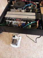
Finally, the parts arrived! This modification will improve the distortion figure and will allow more control of the bias current.
The first amplifier module is ready from the VBE Multiplier modifications. Testing it with a feeble split power supply, has shown it is underbiased. The bias current per pair is too low. Notwithstanding of all this, when a signal was applied it amplified a music signal without any noticeable distortion. I expected to hear the harhness of crossover distortion, but I didn't. Irrespective of playing these particular music tracks corrected, I am still intent on biasing it correctly at around 12mA per pair. There are four pairs, {2SC5200, 2SA1943}, which contribute to a collective bias current of 48mA. Across a 0.1Ohm resistor this has to result in a potential difference of 48x10^-3*0.1 = 4.8mV.
As the amplifier module is combersome to work on, I will apply an extra resistor in parallel with the 590R base-emitter resistance. This will increase the multiplier voltage.
As the amplifier module is combersome to work on, I will apply an extra resistor in parallel with the 590R base-emitter resistance. This will increase the multiplier voltage.
The negative feedback is working hard to "fix" crossover distortion.
22mV across a 0.1 ohm resistor gives a bias current of 220mA total for the four pairs. This is high. 0.1 ohms is too small for good thermal stability.
Ed
22mV across a 0.1 ohm resistor gives a bias current of 220mA total for the four pairs. This is high. 0.1 ohms is too small for good thermal stability.
Ed
You don’t need very much bias current at all to get rid of immediately-obvious crossover distortion. A couple of mA and it goes from sounding like a mistuned FM radio to “clean”, but going to 20 or 30 mA will improve the overall spectrum. Also EF3’s can get away with significantly less bias than EF2‘s for a given amount of crossover distortion.
The output stage of this amplifier is of CFP type. The driver stage is a push-pull stage feeding resistors at the rails. These resistors provide the driving voltage for the output pairs. All transistors in the output stage have 0.22R emitter resistors.
Using two additional signal diodes and a resistor, the bias current should be more readily controllable. In fact, I can say, this has been achieved as I can control the bias current to the nearest milliampere. However, I do not know how the bias current will vary with temperature rise. The simulations show it should not be very high compared to lower temperatures.
Using two additional signal diodes and a resistor, the bias current should be more readily controllable. In fact, I can say, this has been achieved as I can control the bias current to the nearest milliampere. However, I do not know how the bias current will vary with temperature rise. The simulations show it should not be very high compared to lower temperatures.
I think that wg_ski's post #34 hit the nail on the head. The CFP output transistors just add current gain to the driver transistors. You want to stabilize the driver transistor current. The Vbe multiplier should be near the drivers. Remove D10-12. R21 and R24 are too small for good thermal stability. These should be in the range of 0.22-0.33 ohms.
Since you have run simulations, you know the range of bias currents. You only need to ensure that the lower end is at or above the optimal for lowest distortion, and the upper end is far away from the maximum allowable dissipation.
Ed
Since you have run simulations, you know the range of bias currents. You only need to ensure that the lower end is at or above the optimal for lowest distortion, and the upper end is far away from the maximum allowable dissipation.
Ed
The solution to get a better bias current through the output transistors was to decrease the 590R resistance to ~540R. Now, the cumulative bias current for four output transistors is 48mA. This means every transistor in the ouput is consuming 12mA. Since, this channel passed the test, I installed it back inside its amplifier box and did the bulb test at 120V AC mains voltage. In am in the EU with a mains voltage of 230V AC. As I will most probably never need the amplifier full power output, I will use a much reduced 'mains' voltage. In fact, I have a step down transformer fitted in an insulated box with an output of 48V AC. This is more than enough for my needs. I have discovered like some people on these fora, that even 1W RMS is loud in a home environment.
Please be aware, this amplifier is a substantial modification of the Wharfedale S1500 amplifier and I do not have a lot of space to do whatever I decide. Modified and working with a rail voltage of around 12V DC: this amplifier already gave me more than a year of good service. I re-opened it because it was showing signs something was wrong and I knew the VBE multiplier pots were low quality and could be failing. This change also improved the total hormonic figure by a factor of around 10. The original circuitry had a THD of 0.5%. Now it has around 0.003%.
From the original Wharfedale S1500 I kept:
a) the power supply
b) the smoothing capacitor stage
c) the power stage and driver stage
d) the input and output PCBs. The input PCB was modified to suite the new changes.
I removed the rest which was implemented in SMD technology.
Thanks to all who contributed.
Finally, all the changes have been implemented. One channel has a DC offset just below 1mV and the other around 10mV. Maybe the differential pair were not from the same batch. I did the filament bulb test for both channels installed in their amplifier box and using the amplifier power supply. The stability of the filament yellow-orange glow shows the bias must be stable.
Attachments
- Home
- Amplifiers
- Solid State
- Diodes and VBE multipliers.