What do you mean by presets?
I use the Vbe multiplier ckt with the pot across the b-e if the pot wiper opens you have minimum bias which is your safety. If you use a pot in series with diodes then if the pot wiper fails you get max bias which is a problem
I think we have covered most of the subject. You have not even posted a schematic so far so we are discussing general usage with no specifics
Multi-turn pots such as these - they don’t fail or get noisy/intermittent since they are designed for application where millivolts or microvolts matter. Still a good idea to put it in the base-emitter with the wiper tied to one end, and in series with a fixed resistor such that minimum ohm setting can’t go to zero between base and emitter.
Well, you can’t say that they NEVER fail - when you short out the output transistors due to second breakdown you CAN kill the bias stack and perhaps the pot because you could get full Vcc across it. Which is why you check these parts first when you do replace a set of outputs/drivers. But a good pot like this will never be the cause of failure where a cheap carbon one can.
Well, you can’t say that they NEVER fail - when you short out the output transistors due to second breakdown you CAN kill the bias stack and perhaps the pot because you could get full Vcc across it. Which is why you check these parts first when you do replace a set of outputs/drivers. But a good pot like this will never be the cause of failure where a cheap carbon one can.
Attachments

I can't confirm this.I am thinking of two or more diodes with a high resistance shunt used as a bias voltage trimmer. Diodes have the advantage of becoming shorted in the event of failure as opposed to a VBE transistor which may become open circuited causing the bias voltage to increase to damaging values. I am thinking about using rectifier diodes as bias diodes.
Help is much appreciated.
Open circuit in the Vbe multiplier means maximal possible current of power supply goes through the output devices.
Consequence is in most cases the damage of this parts, the driver stage of power buffer, various burned resistors and sometimes parts of the VAS-stage and Vbe multiplier itself.
But until now I haven't found a transistor of Vbe multiplier with open C-E pad as a reason for damaged output transistors.
Please note: There are Vbe multiplier circuit topologies relatively often to find with a great deficiency :
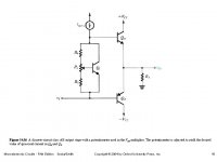
Potentiometer is located in the CB-pad (instead in the BE pad) of the transistor from Vbe multiplier or the base lead is only connected with the middle pin of potentiometer resp. variable resistor (like from first attachment).
Any contact issue (e. g. corrosion oxidation) of this variable resistor leads to the maximum possible current flow through the output stage with this topology. For this reason I modify always such Vbe multiplier circuit topology in a way that exactly the opposite happens in case of contact issues, namely no current flow in the output stage (i. e. idle resp. quiescent current = zero).
There are also different variants with only diodes:
1) integrated circuit resp. diode array with three or four diodes in serial connection built in in one part and special outlines
e. g. SANKEN STV-3h or STV-4h for heatsink mounting
https://audiokarma.org/forums/index.php?threads/sanken-stv3h-y-testing-and-installation.822754/
https://www.diyaudio.com/community/threads/stv-4h-and-stv-3h-diodes-array.83778/
or the vintage ZTE-Series, also often to find - especially in German solid state amplifiers from the late 60th - unfortunately not for heatsink mounting
https://pdf1.alldatasheet.com/datasheet-pdf/view/102647/VISHAY/ZTE2.4.html
Please note - some young guys think, a good currently replacement are zeners.
From my view this isn't possible.
2) single diodes in series like 1N3754 - go to page 37 under
https://pdf1.alldatasheet.com/datasheet-pdf/view/1164334/ETC1/1N3754.html
https://www.vintage-radio.net/forum...9023b9389c88&attachmentid=122364&d=1459814491
https://www.vintage-radio.net/forum/showthread.php?t=125287
Both versions I don't like to maintained the genuine condition and I make in most cases exactly the opposite to your approach as described here:
https://electronics.stackexchange.c...hat-can-i-use-to-replace-an-sv-04f-bias-diode
Stability of idle current with only diodes are only present in cases, where additional NTC is in use like in the circuit from last attachment
Attachments
Last edited:
I use 2 diodes series a pot on the AX6. Mounted over the remote output transistors which are off the driver board on the heat sink in my 1966 design chassis. I clamp the pot with a parallel schottky diode. With no pot, the O.T. idle bias is ~40 ma. with pot, 20 ma. No great tragedy if the pot wiper loses contact.
Thanks to all for all your replies.
The amplifier I am writing about suffers from an unstable quiescent current which varies very substantially as temperature changes. It is also fluctuating considerably for a reason I did not yet understand. The VBE multilpier pot is of the carbon type and does not look like a serious product but a cheap one. The output stage is of the complementary feedback type with the exception that the driver stage is an emitter follower connected as usual. Since, there are only two emitter-base junctions to bias using the VBE multiplier, the multiplication factor of the multiplier is slightly below 2. While this may suffice for the driver stage itself to keep it stable, it cannot do anything to the output pairs to keep the quiescent current under control when the temperature changes. More aggressive control of the driver stage is needed, and this is achieved by setting the multiplying factor to almost 4. A factor of 4 means a higher VBE multiplier voltage, which can be counteracted by using signal diodes in the based paths of the driver stage. To achieve almost complete temperature independence up to a temperature of 80C, I had to add three signal diodes two to one driver transistor and one to the other. Using two or four signal diodes, did not produce proper temperature independence.
Since, one driver transistor has a substantially lower beta compared with the other, I used two signal diodes in series with the base of the transistor having the higher gain. This was done in an attempt to compensate for breaking the symmetry.
To suppress severe switching ringing in the signal diodes feeding the drivers' transistor bases, I had to use shunting 5n6F capacitors across the added diodes. With these capacitors no ringing takes place and the distortion figure is slightly better compared to without them.
Please note, this amplifier gave me already a service of two years practically without issues, but the rails were limited to only about 15V DC. This low voltage may have prevented the amplifier from destroying itself with such a vulnerable quiescent current bias.
Attachments
For me the most interesting questions in this case are the follow!Thanks to all for all your replies.
The amplifier I am writing about suffers from an unstable quiescent current which varies very substantially as temperature changes. It is also fluctuating considerably for a reason I did not yet understand. The VBE multilpier pot is of the carbon type and does not look like a serious product but a cheap one. The output stage is of the complementary feedback type with the exception that the driver stage is an emitter follower connected as usual. Since, there are only two emitter-base junctions to bias using the VBE multiplier, the multiplication factor of the multiplier is slightly below 2. While this may suffice for the driver stage itself to keep it stable, it cannot do anything to the output pairs to keep the quiescent current under control when the temperature changes. More aggressive control of the driver stage is needed, and this is achieved by setting the multiplying factor to almost 4. A factor of 4 means a higher VBE multiplier voltage, which can be counteracted by using signal diodes in the based paths of the driver stage. To achieve almost complete temperature independence up to a temperature of 80C, I had to add three signal diodes two to one driver transistor and one to the other. Using two or four signal diodes, did not produce proper temperature independence.
Since, one driver transistor has a substantially lower beta compared with the other, I used two signal diodes in series with the base of the transistor having the higher gain. This was done in an attempt to compensate for breaking the symmetry.
To suppress severe switching ringing in the signal diodes feeding the drivers' transistor bases, I had to use shunting 5n6F capacitors across the added diodes. With these capacitors no ringing takes place and the distortion figure is slightly better compared to without them.
Please note, this amplifier gave me already a service of two years practically without issues, but the rails were limited to only about 15V DC. This low voltage may have prevented the amplifier from destroying itself with such a vulnerable quiescent current bias.
1) What happens, if you disconnect completely the output power devices of the CFP/Sziklai darlington (i. e. only the MJE15030/15031 are in operating) ?
If the voltage between the 22R resistor (actually the BE voltage of each output device) is stable independent of the ambient temperature, the output devices are not close enough to it'*s specification. Otherwise the reason is around the Vbe multiplier - so I think.
2) The attempt to compensate different hfe of the driver transistors by additional diodes in the signal pad to one of it's base leads is new for me. From where you have found this approach ?
In post #64 under
https://www.diyaudio.com/community/...us-vbe-multipliers.117047/page-4#post-7000659
I have post all information on diyaudio concerning Vbe multiplier - maybe there are additional helpful advices.
The additional diode in the signal pad of one of the driver transistors is not intended to compensate for a different hfe. The decisive reason is to require a sufficiently high VBE multiplier voltage, so that, changes in Vbe are amplified by around a factor of 4.

Replies suggest diode biasing is advantageous in the design of integrated circuits where thermal coupling and component area can be adjusted. In my case, diodes are more difficult to thermally couple because of lack of space. Therefore, I will take the advice of the many who are advocating the use of a VBE multiplier which must provide a good and stable bias and compensate for temperature changes. The quiescent current must remain constant throughout the operating temperature range.
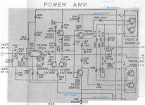
The schematic I am posting has a bias which does not change with temperature although at around 80C there is an bias current increase of a few milliamps per output pair.
The schematic I am posting has a bias which does not change with temperature although at around 80C there is an bias current increase of a few milliamps per output pair.
Attachments
Read post 24 sentence 2. You clamp the pot with a parallel schottky or germanium diode, or silicon if appropriate. Then measure the idle current with no pot at all. If not okay without pot, (twice normal) use a parallel resistor. I've seen a lot more shorted & open transistors than diodes in my repairs.I see absolutely no reason to use a diode stack over a transistor based VBE multiplier... if any of the diodes or the pot go open, your output stage is toast.
Only open diodes I've seen were in a temp sense circuit that had 170 v from 10000 uf rail caps burn through it from shorted output transistors. Manufacturer had diodes in a milled slot in the O.T. heat sink covered in heat conductive glue.
This is diy audio: we don't have to worry about spending $.06 extra for a "what if" part and losing market share to the competition.
Last edited:
Thanks to all for all your replies.
The amplifier I am writing about suffers from an unstable quiescent current which varies very substantially as temperature changes. It is also fluctuating considerably for a reason I did not yet understand. The VBE multilpier pot is of the carbon type and does not look like a serious product but a cheap one. The output stage is of the complementary feedback type with the exception that the driver stage is an emitter follower connected as usual. Since, there are only two emitter-base junctions to bias using the VBE multiplier, the multiplication factor of the multiplier is slightly below 2. While this may suffice for the driver stage itself to keep it stable, it cannot do anything to the output pairs to keep the quiescent current under control when the temperature changes. More aggressive control of the driver stage is needed, and this is achieved by setting the multiplying factor to almost 4. A factor of 4 means a higher VBE multiplier voltage, which can be counteracted by using signal diodes in the based paths of the driver stage. To achieve almost complete temperature independence up to a temperature of 80C, I had to add three signal diodes two to one driver transistor and one to the other. Using two or four signal diodes, did not produce proper temperature independence.
Since, one driver transistor has a substantially lower beta compared with the other, I used two signal diodes in series with the base of the transistor having the higher gain. This was done in an attempt to compensate for breaking the symmetry.
To suppress severe switching ringing in the signal diodes feeding the drivers' transistor bases, I had to use shunting 5n6F capacitors across the added diodes. With these capacitors no ringing takes place and the distortion figure is slightly better compared to without them.
Please note, this amplifier gave me already a service of two years practically without issues, but the rails were limited to only about 15V DC. This low voltage may have prevented the amplifier from destroying itself with such a vulnerable quiescent current bias.
In my experience, poor thermal coupling between sensing element (Vbe multiplier transistor) and the power transistors is often the reason for instable quiescent current. Make sure it is mounted as close as possible to the output transistor so the time lag is minimal. Otherwise you end up with some sort of thermal self-oscillation.
There should always be a buffer for this process though, an efficient heatsink that can keep the output trz relatively cold even with a wrong bias long enough and a copper interface is pretty much welcome .
There are four 2SC5200-2SA1943 pairs in the output. Does mounting the VBE multiplier sensing transistor on any output transistor solve the issue of thermal oscillations?
If I have to mount the sensing transistors on the back of two output transistors, I can opt to use a VBE multiplier employing two transistors in such a way, that the voltage is about four times VBE. I have read about an attractive multiplier which only allows the multiplier's voltage to vary only by a little amount around 4*Vbe.
If I have to mount the sensing transistors on the back of two output transistors, I can opt to use a VBE multiplier employing two transistors in such a way, that the voltage is about four times VBE. I have read about an attractive multiplier which only allows the multiplier's voltage to vary only by a little amount around 4*Vbe.
Last edited:
D10-12 may be the problem - they are really unnecessary and making THEM run at the same temp as the vbe multiplier, drivers, and outputs is next to impossible. The output is a CFP, where the vbe multiplier needs to sense the temp of the DRIVERS more than it does the outputs anyway. Anything else in the loop (besides the emitter resistor which you need) is detrimental. Iq is sensitive to changes in vbe of the driver, and there is still some additional dependence on output beta which also increases with temp (near the Q point anyway). So it’s best to put ALL the drivers and outputs on one heat sink, and put the Vbe mult closest to the driver physically. If it’s still unstable increase R21 and R24. If you can’t do that you need a bigger heatsink.
These diodes allow the use of a multiplication factor of around 4, without them the multiplication factor would be around 2, which is too low according to my simulations. The whole idea of my setup is to overcompensate the drivers for temperature changes so that the overcompensation is countered by increases in beta of the output devices. This results in a quiescent current that is independent of operating temperature.D10-12 may be the problem
Diodes D10 to D12 will reside on a PCB and will not be subjected to the temperature of the output stage.
I will simulate further to use four diodes instead of three to retain driver symmetry. My choice of a VBE multiplier is to use two complementary sensing transistors.
Use the highest available hfe type for Vbe multiplier. I use TTC004B with hfe>200, but there is special bjt for this function: 2SC4495 with hfe>500.
I simulated the amplifier with a VBE multiplier employing two transistors with both transistors carrying the same current. The multiplication factor is about 4, but simulations have shown that thermal compensation is inferior to my previous version using only one transistor as a VBE multiplyer and three signal diodes to compensate for the extra biasing voltage. The previous circuit simulates better.
Recepy for oscilations: high open loop gain and low bandwidth i.e. lag. In this thermo-electrical system.I simulated the amplifier with a VBE multiplier employing two transistors with both transistors carrying the same current. The multiplication factor is about 4, but simulations have shown that thermal compensation is inferior to my previous version using only one transistor as a VBE multiplyer and three signal diodes to compensate for the extra biasing voltage. The previous circuit simulates better.
If my memory serves me right, there is a version of the basic simple VBE multiplier circuit which can achieve both low voltages like 1.2V, and high gain, like a factor of 4 or more. As far as I remember, a stable DC voltage is inserted between the resistor connected between the emitter and base. This results in any changes in VBE due to temperature changes to appear across the mentioned resistor. Since, the latter uses a lesser voltage compared to without the series voltage source, the resulting amplifying factor is bigger.
Post Scriptum:
I tried this, but the gain of the VBE multiplier does not cancel thermal changes in the quiescent current completely.
The more I try, the more I am getting the impression all this trouble is due to the way the output stage is built with the transistors' emitters next to the rails. It seems pure emitter follower output stages are much more well behaved compared to CFP based output stages.
Last edited:
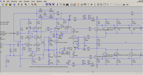
I reverted back to the schematic employing three signal diodes in the driver transistors' base paths. To get rid of symmetry breakage, I removed one signal diode and added two Schottky diodes, one per driver base. This restored symmetry and the temperature compensation is still very close to ideal. The quiescent current increases to about 24mA per pair at a temperature of 80C. At 60C, the increase is far less pronounced.
Attachments
- Home
- Amplifiers
- Solid State
- Diodes and VBE multipliers.