I beg everyone's pardon for posting again.
Measurement from LTSpice simulations show that to compensate for temperature changes and keep a stable quiescent current, my amplifier needs an amplification factor of 3.56Vbe. The measured Vbe is 630mV. Since, I understand diodes have a fixed characteristic and increasing voltage across them is quite difficult much unlike a BJT, I am still tempted to continue my search for a diode biasing scheme. However, a factor of 3.56 is quite difficult to satisfy. In my inexperienced opinion, as this is the first time I am looking seriously at biasing an amplifier using diodes, three diodes would be needed, but that leaves out a factor of 0.56 which is still needed.
Some calculations: (not an expert here!)
3.56Vbe = 3.56*0.63V = 2.24V (correct to 2 d.p.)
The VAS works at 13.8mA.
Any suggestions as to how this can be achieved with real diodes which can be mounted onto a heatsink? I like the idea of using a small series resistance with a Schottky diode across it.
This post is another VBE multiplier configuration that compensates for temperature changes. The bias remains almost constant throughout 25C to 80C. This time, the circuit uses a BD139 transistor and a resistance which drops by 1.667R for every degree Celcius increase. I have NOT yet found a way to implement such a resistance. The inherent advantage over the previous circuit is this time temperature is sensed at two points instead of only one. Another advantage is this circuit does not use additional diodes and bypassing capacitors to suppress switching ringing at the driver bases.
This circuit seems to be another possibility of compensating for temperature changes and having a stable bias. This is the second solution and seems to be more attainable than the previous one.
This circuit seems to be another possibility of compensating for temperature changes and having a stable bias. This is the second solution and seems to be more attainable than the previous one.
Attachments
Hi edbarx,
Your latest circuit (Post 42 above) can be stabilized using the Vbe multiplier and without a thermistor by raising the the Vbe multiplier voltage to 2.5V. See attached circuit.
I have added two 1N4148 diodes to the bases of Q13, Q14 with a 470 R for 2.7mA through these diodes. They run at ambient.
Then the Vbe multiplier is mounted in such a way to see 80% of the temperature rise of Q13, Q14. This is a "thermal attenuation" factor of 0.8 (see Bob Cordell's book for calculations). One way to drop the temperature of the Vbe multiplier slightly is to use several thermal washers between the Vbe multiplier and the heatsink for Q13,Q14. Or several pads cut from some PCB? I find bench trials are needed as simulation models and calculations cannot give enough accuracy for this situation.
Keep up the good work,
Ian
Attachments
Thank you so much for taking the time to edit my amplifier circuit and simulate it to improve it. Your circuit uses a temperature factor 0.8, which means with a factor of 1.0 there is over compensation for temperature. This gave me the possibility of using a factor of 1.0 and employ a thermistor to slightly drop the multiplier's resistance between the negative end and its base. Using a simple calculation for parallel resistors and the thermistor's resistance at 25C and 80C, I placed a resistor R in parallel with a resistor r in series with the thermistor. The objective was to emulate the required values of resistance across the BE junction that produce the right bias at 25C and at 80C. Simulations showed that between these temperatures and at temperatures below 25C, the bias remains very near to what is needed.
Again thanks, as your post made it possible for me to get rid of using an auxiliary control circuit to drive an optocoupler connected to the base emitter junction of the multiplier. The latter solution (my solution) is more complicated and hence more prone to error and malfunction.
I am attaching two schematics. One is your contribution with my edits to add a thermistor and get rid of having to use a factor of 0.8, and the other is my version which is clearly far more complicated and difficult to test and implement.
Knowing I can use a thermistor and keep the schematic simple and free of an auxiliary circuit, I will now try to calculate resistance values which are more attainable.
The calculation:
Code:
At 25C Reb = 505 Ohm, R thermistor = 10000 Ohm
At 80C Reb = 470 Ohm, R thermistor = 1662.4 Ohm


     |---R----|
-----|        |------
     |--r---t-|

1/505 = 1/R + 1/(r + 10000).....(1)
1/470 = 1/R + 1/(r + 1662.4)....(2)

Subtracting (1) from (2):
1/470 - 1/505 = 1/(r + 1662.4) - 1/(r + 10000)
0.00014746 = {(r + 10000) - (r + 1662.4)} / {(r + 1662.4)(r + 10000)}
0.00014746 = 8337.6/{(r + 1662.4)(r + 10000)}

Rearranging:
(r + 1662.4)(r + 10000) = 56541435
r^2 + 11662.4r + 16624000 = 56541435
r^2 + 11662.4r - 39917435 = 0

Solving gives two solutions, one negative (impossible) and  one positive:
r = 2766.49 Ohm

Using r in either (1) or (2) gives:
R = 525.80 ohm
Attachments
Last edited:

Searching for resistor values online, it is clear the resistor values themselves are not a problem if I use resistors in series. I think, the VBE multiplier will require the usual potentiometer and another one in series with the thermistor. Both potentiometers should be low value like 100R or so.
The setup can be done around 1pm because at that time the ambient temperature usually reaches a plateau. The temperature of the heatsink will be read together with the quiescent current from simulations for the heatsink temperature. The effective resistance in series with the thermistor will be set to agree with the calculated value. The VBE multiplier pot will then be used to set the quiescent current to agree with the simulated value. After this setup, the temperature will be allowed to change a little to further observe what happens to the quiescent current.
If there is a better procedure compared with the above, I am ready to use it.
This is a practical question relating to thisn same thread.
Many thermistors are like ceramic capacitors without any mounting means apart from having two wires. I would like to ask what members of these forums do to achieve a good and secure thermal contact between heatsinks and thermistors. One possible way that comes to my mind is to use a metal strip, fold an end, and with a flat screwdriver bit, make some space for a thermistor which is placed inside this space. The latter, is filled with heatsink grease.
Many thermistors are like ceramic capacitors without any mounting means apart from having two wires. I would like to ask what members of these forums do to achieve a good and secure thermal contact between heatsinks and thermistors. One possible way that comes to my mind is to use a metal strip, fold an end, and with a flat screwdriver bit, make some space for a thermistor which is placed inside this space. The latter, is filled with heatsink grease.
Hi Ed,
But the chip is fragile. I accidentally broke the plated end off the thermistor when I bumped the flying lead. I think the chip needs a supporting thin, very small PCB to strengthen the termination and make it easier to solder to a TO-220 lead. Maybe cut something from a discarded flexible PCB (the orange Kapron type).
There are also MELF SMD thermistors eg here. They are in a glass-case and are robust and hand solderable to a TO-220 or whatever lead. But not a large resistance range in stock.
SMD thermistors are available. I soldered one to a TO-220 middle lead at the exit of the epoxy case. To the other end of the thermistor I soldered a thin wire (about 0.3mm dia). It worked well, thermally very fast. Tricky to hand solder with an 0805 chip.Many thermistors are like ceramic capacitors without any mounting means apart from having two wires.
But the chip is fragile. I accidentally broke the plated end off the thermistor when I bumped the flying lead. I think the chip needs a supporting thin, very small PCB to strengthen the termination and make it easier to solder to a TO-220 lead. Maybe cut something from a discarded flexible PCB (the orange Kapron type).
There are also MELF SMD thermistors eg here. They are in a glass-case and are robust and hand solderable to a TO-220 or whatever lead. But not a large resistance range in stock.
Is the VAS section stable enough to handle higher voltage rail? The reason I asked because you are using fast transistors and I see a lot of compensation (phase network?), your output stage is CFP (pretty sensitive with unstability issues). With my experience CFP seems to favor a simpler VAS scheme thus making VBE response more controllable.
While performing more simulations for a list of temperatures, I very sadly discovered the output oscillates at 2MHz with a peak voltage of about 0.25V when no signal is applied to the input. Increasing the Miller Capacitance to 120pF seems to solve the issue of self oscillations.
More simulations are required.
More simulations are required.
Dear edbarx,Since integrated linear amplifiers may use a pair of diodes instead of a VBE multiplier, I would like to ask whether anyone had tried successfully using diodes instead of a VBE multiplier to bias a Class AB amplifier built from discrete components. I am thinking of two or more diodes with a high resistance shunt used as a bias voltage trimmer. Diodes have the advantage of becoming shorted in the event of failure as opposed to a VBE transistor which may become open circuited causing the bias voltage to increase to damaging values. I am thinking about using rectifier diodes as bias diodes.
Help is much appreciated.
Vbe multipliers seldom fail, especially open. The main advantage is they're easily tweaked for such things as 1.5 Vbe's. If you want tweakable diodes, you can always mix Silicon diodes and Schottkys. I've used all the above.
Rectifier diodes and Rectifier Schottkys work fine. They almost always fail-safe shorted. One thing - you have to be careful the bias circuit's thermal time constant should match the output devices. Epoxy or thermal-grease the diodes to the output devices or their heat sinks.
If you're really insane, you can use a modded Bandgap regulator and tweak its tempco to match the tempco of the output transistor Base-Emitter junctions.
If you're going to use a tweak pot, always be sure if its wiper gets cruddy, etc, and the pot looks "open-ish", the crossover circuit fail-safes in low LV mode, not HV.Since integrated linear amplifiers may use a pair of diodes instead of a VBE multiplier, I would like to ask whether anyone had tried successfully using diodes instead of a VBE multiplier to bias a Class AB amplifier built from discrete components. I am thinking of two or more diodes with a high resistance shunt used as a bias voltage trimmer. Diodes have the advantage of becoming shorted in the event of failure as opposed to a VBE transistor which may become open circuited causing the bias voltage to increase to damaging values. I am thinking about using rectifier diodes as bias diodes.
Help is much appreciated.
Dear JMFahey,That is quite unrealistic if we are speaking of power transistors..
Re is selected to offer some thermal stability , to make multiple transistors share current evenly and even to sample current to trigger short protection, and as low value as possible, hence the typical 0.22 0.33 up to 0.47 ohm values chosen.
It is NOT a Bias adjustment system by any means and nobody ever used them for that.
The proper Bias system is to control applied Vbe , to make it temperature sensitive, and if possible: adjustable.
The problem with plain diode biasing is that it´s adjustable in "1 diode" steps (duh) while Vbe multipliers allow for fine adjustment to any value.
Diode bias adjustments are quite crude by comparison.
Never say "nobody ever used them". I've been bitten in the butt doing or saying just that.
In the dark ages, I needed 30 milliOhm Emitter equalizing resistors to match banks of 10 NPN, 100 Watt GE power Darlingtons @ 20 Amps each, in a Patented 30 kW Class G MRI Gradient supply. Class G and H didn't even have names until years later.
The resistors had to be mechanically self-supporting and have the proper positive temperature coefficient. 16 gauge Iron was perfect. I wrapped some steel coat hangers around a 1 inch dowel, found which dry cleaner had provided the coat hangers, and located the coat hanger company's steel wire vendor. We had them coiled, then Cad plated, when it was still legal, then soldered on spade lugs. Many years later, I still have two somewhere. The neat thing - if a transistor went into thermal runaway, its coat hanger Emitter resistor turned blue. You instantly knew which Darlington had failed. They almost always failed by melting into blobs of Silicon.
Schottkys make nice 1/3 or 1/2 diode tweaks. Their tempcos are still close to Silicon diodes. If I recall, someone like National Semi actually sold a "smart" crossover IC.
Nice application but we are talking biasing here.
You are talking current equalizing , a very different use.
As a side note, you are talking 20A current levels, OP is talking milliamps.
You are talking current equalizing , a very different use.
As a side note, you are talking 20A current levels, OP is talking milliamps.
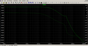
Using more simulations the Miller Compensating Capacitor was increased to 180pF. This produces a gain of 0dB at 2MHz. The distortion figure does not seem to be affected by this increase. The input voltage was set to 1 V (peak value) for convenience.
The attached LTSpice screenshot shows the AC analysis. Comments are most welcome as changing the value of the Miller capacitance profoundly affects stability.
Note:
I am going through all this, because, I need to know what parts to order, so that I include them in one order preferably from the same supplier.
Attachments
For reasons of mounting and a good thermal contact, I am thinking about using a TO 220 packaged transistor. This should allow me to mount the VBE multiplier transistor over one of the 2SA1943 or 2SC5200 transistors. The same fixing bolt will be used. However, I think, as these large transistors are packaged in a plastic body, there will be some thermal lag between the VBE multiplier transistor and output transistors. The fixing bolts are made of stainless steel. {For reference, see my enlarged avatar. The power transistors are the black things fixed onto the heatsink.}
Ed, if extending the bandwidth does not increase the available gain at up to 20kHz, there is no change in distortion.Using more simulations the Miller Compensating Capacitor was increased to 180pF. This produces a gain of 0dB at 2MHz. The distortion figure does not seem to be affected by this increase. The input voltage was set to 1 V (peak value) for convenience.
The attached LTSpice screenshot shows the AC analysis. Comments are most welcome as changing the value of the Miller capacitance profoundly affects stability.
Note:
I am going through all this, because, I need to know what parts to order, so that I include them in one order preferably from the same supplier.
In such a case, extending the bandwidth may not be a good thing. Think opening a window further - more junk flies in.
Jan
Thanks for the advice. Extending the bandwidth into ultrasound and radio frequencies is riskky as it asks for more instances of instability through difficult to detect parasitic paths. I increased the Miller Capacitance erroneously as I was too tired with repeated simulations. There is no need of increasing this crucial capacitance.jan.didden said:Ed, if extending the bandwidth does not increase the available gain at up to 20kHz, there is no change in distortion.
My aim is now to find two suitably mountable transistors to act as VBE multipliers. I assume, the transition frequency, Ft, does not need to be very high for a VBE multiplier, but the transfer ratio should be large. I found that 2SC2575 has an Ft of 180MHz and hfe of 150 at 300mA. This is packaged in a TO220 package and is available. The datasheet is available but LTSpice does not recognise it. From the datasheet it should be possible to define 2SC2575 so that LTSpice would be able to simulate it, but I do not know how to do it although I have an idea.
Last edited:
2SC4495 developed fot Vbe multiplier application. But i use the TO-126 packaged TTC004B, which works quite well in this position.Thanks for the advice. Extending the bandwidth into ultrasound and radio frequencies is riskky as it asks for more instances of instability through difficult to detect parasitic paths. I increased the Miller Capacitance erroneously as I was too tired with repeated simulations. There is no need of increasing this crucial capacitance.
My aim is now to find two suitably mountable transistors to act as VBE multipliers. I assume, the transition frequency, Ft, does not need to be very high for a VBE multiplier, but the transfer ratio should be large. I found that 2SC2575 has an Ft of 180MHz and hfe of 150 at 300mA. This is packaged in a TO220 package and is available. The datasheet is available but LTSpice does not recognise it. From the datasheet it should be possible to define 2SC2575 so that LTSpice would be able to simulate it, but I do not know how to do it although I have an idea.
I beg everyone's pardon for posting again.
Measurement from LTSpice simulations show that to compensate for temperature changes and keep a stable quiescent current, my amplifier needs an amplification factor of 3.56Vbe. The measured Vbe is 630mV. Since, I understand diodes have a fixed characteristic and increasing voltage across them is quite difficult much unlike a BJT, I am still tempted to continue my search for a diode biasing scheme. However, a factor of 3.56 is quite difficult to satisfy. In my inexperienced opinion, as this is the first time I am looking seriously at biasing an amplifier using diodes, three diodes would be needed, but that leaves out a factor of 0.56 which is still needed.
Some calculations: (not an expert here!)
3.56Vbe = 3.56*0.63V = 2.24V (correct to 2 d.p.)
The VAS works at 13.8mA.
Any suggestions as to how this can be achieved with real diodes which can be mounted onto a heatsink? I like the idea of using a small series resistance with a Schottky diode across it.
Dear edbarx,
The VBE multiplier is the simplest way to get the required Voltage. Remember, when you multiply the VBE with a multiplier, you also multiply the base-emitter's negative tempco (miiliVolts per degree C ). Using several series-connected diodes from differing technologies may also give you a different tempco. If I recall, a Schottky, like a BAT-54, has a different negative tempco than a Silicon signal diode, like a 1N914.
Ideally, if the VBE multiplier is directly driving a bank of several NPN/PNP output devices, you'd prefer the VBE multiplier's tempco match the output bank's' 2 tempcos. If you use series connected diodes and pad up the forward voltage with a small series resistor, you decrease the effective tempco. Imagine using a large padding resistor, like hundreds of Ohms - you virtually eliminate the desired negative tempco, since most common resistors have tempcos many times lower than forward-biased diodes.
Rather than trying to match thermal time constants by bolting two heat sinks together, I'd use a VBE multiplier with something tiny, with a short thermal time constant like a MMBT2222. and bond it to the heat sink of one the power devices it's driving, using thermal epoxy. Better yet, use JB Weld. It has excellent thermal characteristics and it's available almost everywhere. While steel-filled JB Weld is a poor electrical conductor, I'd stay away from the MMBT's leads with the JB Weld.
What you're doing with the tiny device bonded to the power device, is creating an overall thermal time constant that's ~ that of the power device. While the thermal time constant of the power device is, say, 10 seconds, you've bonded a device to it with a fractional-second thermal time constant, so it tracks very well.
- Home
- Amplifiers
- Solid State
- Diodes and VBE multipliers.