Then you cqn try pure Jfet with op1678... seems a good candidate. However a dual. Will be ok with Vunce adaptator without dil8 wocket , solder caps leads surplus direct on the adaptator.What I am going to do, is: start with one psu2, both set to +-5V. Later then switch back to +-5V and +-12V and add a separate+5V for digital part of AD1865 and I will see, if the effort is pays. Cheers
Yeah PCI - USB cards with low jitter TCXO crystals are up to 500 eurosYes, so you have a jittery and not synchronised souce, and you clean it up with cmplicated software / firmware / hardware.
Is that a good solution ? Are there no better solutions ?
Patrick
There is no a motherboard that has USB built-in TCXO of this precision ...
Good idea, even for normal adapter..... solder caps leads surplus direct on the adaptator.
Last edited by a moderator:
"adapter"... sorry.
Made with some UKZ leads 100V : https://www.diyaudio.com/community/...st-tht-i2s-input-nos-r-2r.354078/post-7021918. Easy to take the good diameter when you have tons of caps...ahaha !
Made with some UKZ leads 100V : https://www.diyaudio.com/community/...st-tht-i2s-input-nos-r-2r.354078/post-7021918. Easy to take the good diameter when you have tons of caps...ahaha !
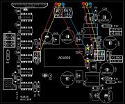
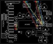
I think there is another cheaper solutionI/V opamps can be powered separately. Don't install J10, J11, J12 and J13. Use these pins for the +-12V PSU:
(+-5V still be needed for the AD1865)
Don't install J1 and J2. Use these pins for the +-5V PSU
Below the connector where it says VA becomes + 12 / -12V
Capacitors C27, C28, C32, C33 change to be 100uF / 16V

great. 😀For the best sound experience avoid direct I2S output from the rpi. Instead use the rpi USB and connect here a high quality USB-I2S device with clean clock (like jlsounds or another xmos based ... I think even the cheap PCM2706 with rpi USB will sound better as direct I2S from the rpi) 😉 ... someone in this thread tried it ...
In the future I can create 40 pins version also for RPI, but it will be the stop-clock 🙂
Last edited:
Recap:
v1. - 1 PSU board (+5, 0, -5 and +12, 0, -12)
v2. - 1 PSU board (+5, 0, -5 and +12, 0, -12) + 1 PSU board (+5, 0)
miro1360 please confirm.
v1. - 1 PSU board (+5, 0, -5 and +12, 0, -12)
v2. - 1 PSU board (+5, 0, -5 and +12, 0, -12) + 1 PSU board (+5, 0)
miro1360 please confirm.
Attachments
Last edited:
Well implemented USB-I2S bridges have separate clock domains for source and DAC. So I2S timings are generated from the same MCK which DAC uses. If the USB-I2S bridge operates with asynchronous (or adaptive) UAC source jitter should have no impact.Yes, so you have a jittery and not synchronised souce, and you clean it up with cmplicated software / firmware / hardware.
Is that a good solution ? Are there no better solutions ?
i found four new unused (still in tube) AD1862 if anyone wants to make me an offer. (bought from Rochester a few years ago i think)
Also two AD1865 - used.
Also two AD1865 - used.
I have one bare AD1862 DAC pcb with onboard FIFO.Would anyone have any AD1862 PCBs and power supply boards to spare?
It's this one, without dac and Xmos.
https://www.diyinhk.com/shop/audio-...fo-reclock.html#/dac-dac_pcb_without_dac_chip
I also have four AD1862
All items in this thread in the Swap Meet forum.
https://www.diyaudio.com/community/threads/ad1862-1865-dac-pcb.387068/
https://www.diyaudio.com/community/threads/ad1862-1865-dac-pcb.387068/
Use v2 😉Recap:
v1. - 1 PSU board (+5, 0, -5 and +12, 0, -12)
v2. - 1 PSU board (+5, 0, -5 and +12, 0, -12) + 1 PSU board (+5, 0)
miro1360 please confirm.
it works with +/-5v, sound beautiful, dont want to put it out, i will try +/-12v later.And Sparkos voltage is minimum +-6V
View attachment 1062440
So whoever tried Sparkos at AD1865 PCB - didn't hear how Sparkos really works ...
what discrete op amp modules are these?it works with +/-5v, sound beautiful, dont want to put it out, i will try +/-12v later. View attachment 1063103
I have to go at least +-10V - since I listen them directly to headphones. Although +-9V is the optimum for Sparkos from datasheet.ss3601.
I've never tried it with + -12, I don't know how much it will heat up.
Last edited:
- Home
- Source & Line
- Digital Line Level
- DAC AD1862: Almost THT, I2S input, NOS, R-2R