@Vunce
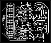
I looked at it. To get a real benefit from smd opamp on the pcb will mean no signal traces underneath this opamp ... and this is not real together with DIL package. It is either one or the another. So we could have one more version with smd opamp alone 😀
I looked at it. To get a real benefit from smd opamp on the pcb will mean no signal traces underneath this opamp ... and this is not real together with DIL package. It is either one or the another. So we could have one more version with smd opamp alone 😀
No problem Miro, I don’t want to burden you.
If you did offer an alternative board with SMD opamp, I would have it fabricated. I’ve tried enough opamps with your original layout to feel comfortable with a direct soldered SOIC8 opamp.
Thank you for considering the idea 🙂
If you did offer an alternative board with SMD opamp, I would have it fabricated. I’ve tried enough opamps with your original layout to feel comfortable with a direct soldered SOIC8 opamp.
Thank you for considering the idea 🙂
Yes, very good, you can order boards))
perhaps there will be no mistake
Attachments

No problem Miro, I don’t want to burden you.
If you did offer an alternative board with SMD opamp, I would have it fabricated. I’ve tried enough opamps with your original layout to feel comfortable with a direct soldered SOIC8 opamp.
Thank you for considering the idea 🙂
Check it three times before ordering 😀
Attachments
Check it three times before ordering 😀
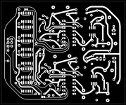
The only thing in the table is that the PIN designations in the plate are not changed, it can mislead people).
GND is now 531 pins and 642 is data-bck-lrck
Opamp legs 2,3,4,6 and 7 all seem to be going to their proper destinations.
Gerbers are downloaded and ready to go in my next pcb order 😀
Thank you Miro!!

Ps: I also noticed a labeling error for the I2S inputs.
GND is now 1,3,5
LRCK = 2
BCK = 4
DATA = 6
Good eyes Traktorist3d 😉
Gerbers are downloaded and ready to go in my next pcb order 😀
Thank you Miro!!
Ps: I also noticed a labeling error for the I2S inputs.
GND is now 1,3,5
LRCK = 2
BCK = 4
DATA = 6
Good eyes Traktorist3d 😉
Last edited:
You are right guys, here is the label correction 🙂
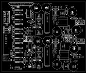
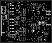
opamp DIL08: diyAudio_AD1862_DAC_v1.3_pad_PPY3_2021-01-14.zip
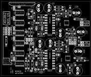
opamp SO08: diyAudio_AD1862_DAC_v1.3_pad_PPY3_SO08_2021-01-14.zip
opamp DIL08: diyAudio_AD1862_DAC_v1.3_pad_PPY3_2021-01-14.zip
opamp SO08: diyAudio_AD1862_DAC_v1.3_pad_PPY3_SO08_2021-01-14.zip
Attachments
-
 AD1862_PCB_v1.3_pad3_so08_TopView.jpg251.2 KB · Views: 1,356
 -
 AD1862_PCB_v1.3_pad3_so08_PartsView.jpg283.4 KB · Views: 1,365
 -
diyAudio_AD1862_DAC_v1.3_pad_PPY3_SO08_2021-01-14.zip663.7 KB · Views: 396
-
 AD1862_PCB_v1.3_pad3_TopView.jpg255.5 KB · Views: 1,381
 -
 AD1862_PCB_v1.3_pad3_PartsView.jpg279.1 KB · Views: 1,371
 -
diyAudio_AD1862_DAC_v1.3_pad_PPY3_2021-01-14.zip670.2 KB · Views: 461
There are DACs with successfuly implemented stopclock method. I did it too in my prototypes and tried to do it as simple as possible. However the simplicity was not the way here, because the stopclock modifies the LRCK. LRCK is the most critical signal in the NOS R-2R (due to possibility of audible jitter) and it should be driven directly from the source. Any further modification is out of the question of simplicity, and the only way is generating the LRCK externally from a precise clock 🙄 This complicates the whole thing so that shift registers become the number one choice for simplicity and efficiency. That's my opinion.
You are right guys, here is the label correction....
Right on!
Thanks Miro 🙂


@nautibuoy
Nice to see your board stacking design and progress information.
If you decide you can then share gerbers for people
Nice to see your board stacking design and progress information.
If you decide you can then share gerbers for people
Yep, more than happy to share the DAC gerbers if it works out.
For the output stage I purchased the PCBs from JIMS Audio;
Borbely balanced tube input mosfet output linestage single ch preamplifier PCB ! - JIMS Audio
I've used this Borbely circuit before with great results. Its a very versatile circuit and I'll be configuring it like the attached diagram. There is a difficulty with this circuit though, the mosfets are a long time out of production and getting genuine parts is a bit of a challenge - fingers crossed that the ones I managed to obtain are genuine.
Of course, there are other options for I/V stages that could be used, I would quite like to try some of bisesik's transformers;
Output transformers for DACs
Attachments
You can get some genuine lateral mosfets from exicon:
Exicon Lateral MOSFETS - Cross-reference Charts
or perhaps the wide known 2sk1058 2sj162
Security Check
Security Check
Exicon Lateral MOSFETS - Cross-reference Charts
or perhaps the wide known 2sk1058 2sj162
Security Check
Security Check
The Mosfets for the Borbely board are Toshiba 2SJ79 and 2SK216
There are seemingly plenty around until you exclude China as a source.
There are seemingly plenty around until you exclude China as a source.
- Home
- Source & Line
- Digital Line Level
- DAC AD1862: Almost THT, I2S input, NOS, R-2R