There is a problem. Your MOSFET models omit both subthreshold conduction and junction capacitance. So your MOSFETs don't show any conduction until 1.825 volts, which is incorrect, and is probably giving you excessively good results. If you have VDMOS models, they can be augmented with ksubthres=0.15 for a crude sanity-check to see the effect of subthreshold conduction.
Thanks, so my model, now
.MODEL ZVN3306 NMOS VTO=1.824 RS=1.572 RD=1.436
+ IS=1E-15 KP=.1233+CBD=35E-12 PB=1
.MODEL N3306D D IS=5E-12 RS=.768
.ENDS ZVN3306
Has to be changed to 1 this
.MODEL ZVN3306 NMOS VTO=1.824 RS=1.572 RD=1.436
+ IS=1E-15 KP=.1233+CBD=35E-12 PB=1 ksubthres=0.15
.MODEL N3306D D IS=5E-12 RS=.768
.ENDS ZVN3306
Or 2 this
.MODEL ZVN3306 NMOS VTO=1.824 RS=1.572 RD=1.436
+ IS=1E-15 KP=.1233+CBD=35E-12 PB=1
.MODEL N3306D D IS=5E-12 RS=.768 ksubthres=0.15
.ENDS ZVN3306
As you can see, models is not my forte (models where from the manufacturers web site).
P.s. If you or anyone else has a better model for this MosFet then please show it here or PM me (I will redo the graphs and show them here)
Last edited:
Those are NMOS models, you need VDMOS models.
The LTspice standard.mos file has many models with subthres or ksubthres, you could find them with a text search.
The LTspice standard.mos file has many models with subthres or ksubthres, you could find them with a text search.
Those are NMOS models, you need VDMOS models.
The LTspice standard.mos file has many models with subthres or ksubthres, you could find them with a text search.
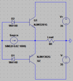
Using this model
*VDMOS with subthreshold (c) Ian Hegglun Feb 2016
.model DN2530-Tjp VDMOS (Rg=1 Vto={-1.50-4.5m*(Tjp-25)} Lambda=8m
+ Rs={0.4*(1+3m*(Tjp-25))} Kp={830m/(1+6m*(Tjp-25))}
+ Ksubthres={0.11} Mtriode={0.15} Rd={2.5*(1+3m*(Tjp-25))}
+ Cgdmax=100p Cgdmin=1p a=0.1 Cgs=170p Cjo=130p
+ m=0.75 VJ=0.75 IS=240p N=1.4 Rb=0.2 )
The simulation shows no problems other than a to low Vgs (for the application)
Is it possible to alter the model so it will show the same Vgs as my selected ZVN3306's exhibit (about 2V(Vds) at 10mA while drain connected to gate [mos-diode-connection] and bjt connected as shown in published schema the DN2530-Tjp shows about 957mV)? if so I will download a complete simulation including the .asc-file.
Attachments

Here a comparison between the two models, the DN2530-Tjp model seems just as viable, for the purpose of soft clipping, as the [faulty] ZVN3306.
Note that I needed to enlarge(multiply) the DN2530-Tjp result by 2.31 to align the graphs.
P.s. here is the BFR340F model
* Model file 'C:\Users\FdW\Electronics\FdW's LTspice Library\NPN\BFR\BFR340F.MOD' created on 'Wednesday, October 15, 2014 10:00:29 AM'.
* by FdWs 'Split And Merge Model File' version '0.9.4813.32841' of 'Tuesday, March 05, 2013'.
* Imported from 'C:\Users\FdW\Electronics\FdW's LTspice Library Source\FdWs.lib' on 'Wednesday, October 15, 2014 10:00:29 AM'.
* by FdWs 'Split And Merge Model File' version '0.9.4813.32841' of 'Tuesday, March 05, 2013'.
.MODEL BFR340F NPN(
+ IS = 2.588E-017
+ BF = 208.3
+ NF = 1
+ VAF = 80.12
+ IKF = 0.1012
+ ISE = 1.921E-015
+ NE = 2
+ BR = 8.99
+ NR = 0.95
+ VAR = 2.277
+ IKR = 0.1924
+ ISC = 3.85E-015
+ NC = 1.5
+ RB = 10.26
+ IRB = 0
+ RBM = 4.697
+ RE = 1.016
+ RC = 5.655
+ XTB = -1.003
+ EG = 1.11
+ XTI = 2.728
+ CJE = 9.724E-014
+ VJE = 0.693
+ MJE = 0.2059
+ TF = 6.027E-012
+ XTF = 12.98
+ VTF = 1.928
+ ITF = 0.04152
+ PTF = 0.1
+ CJC = 1.25E-013
+ VJC = 0.5602
+ MJC = 0.09189
+ XCJC = 0.7499
+ TR = 8.853E-005
+ CJS = 0
+ MJS = 1
+ VJS = 1
+ FC = 0.5
+ KF = 3.4E-10
+ AF = 2.1
+ )
Attachments
Last edited:
Nice to see it works as expected despite the model flaws.
No I was not saying that, I did say 'seems'. And if you are saying that the model has flaws, then you say that the DN2530-Tjp from Ian has flaws.
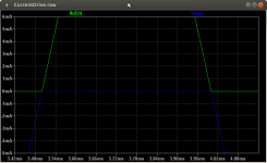
Here it is, one '.asc' sim-file and an picture showing (near) -200dB @ 1.4V input
Yes I know, it is a typical over optimistic simulation result (to be more clear this time)
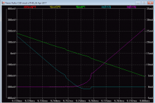
To make this complete, here a set of graphs that shows the effect of the MosFet clipper, all voltages are in RMS, the horizontal straight lines are (top to bottom)
Here a comparison between the two models, the DN2530-Tjp model seems just as viable, for the purpose of soft clipping, as the [faulty] ZVN3306.
One thing would have helped, some positive comment(s), and some help, maybe a model or two, but what I am currently getting is not going anywhere.
Any way, going like this about it is not very helpful, I was just showing something I'm doing (and I like it) and then there was comment about the model, and I am o.k. with that.
The bottom line is, what we are doing now is not making progress in any way, I did get a VDMOS model as requested, and you are still skeptical, why I will never understand, but I give up. It seems not possible to do any good here.
P.s. I would say that the VDMOS model from Ian actually looks better.
Last edited:
I don't know what you got from my previous comment, but I was saying it's nice to see that the circuit still works when you use an accurate model. I know Ian's models are great. Here's a tentative one. It hasn't been fit to the datasheet, but it should be close enough for an assessment.
I do want to help, but I need to understand what you want help for.
I do want to help, but I need to understand what you want help for.
Attachments
Thanks for the updated model I will study it and re-publish the files published before (with the updated model).
There was no help needed, but you did comment on the models used and doubted the functionality of the design by that (model was from the Diodes web site).
From there on information was wanted to resolve the model problem perceived.
Again, thanks for helping to solve this.
There was no help needed, but you did comment on the models used and doubted the functionality of the design by that (model was from the Diodes web site).
From there on information was wanted to resolve the model problem perceived.
There is a problem. Your MOSFET models omit both subthreshold conduction and junction capacitance ...
Those are NMOS models, you need VDMOS models. ...
Again, thanks for helping to solve this.
A simple speed-up idea for the Linear Audio 'CSD' amp
The previous posts are mainly for Wim's new Class-AB topology and there have been some really good ideas so far. Thanks all. Keep up the good work. I think Wim's topology has lots of potential as a top performer.
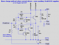
Last week I came up with an idea for removing most of the cross conduction in the Linear Audio 'CSD' amp, and I have bench tested it. I have adapted a turn-off speed-up idea used in solid state relays.
See the attached circuit for the lower side power NPN. A diode, a high gain PNP and a high value resistor can pull down the gate voltage down quickly.
The 0.6V voltage source is needed to generate a small base current in the PNP's (Q1,2) when the drive current stops (otherwise the PNP drops 0.6V from the power transistors Vbe leaving no voltage across the resistor).
This circuit reduced cross conduction current to about 300mA at 100kHz squarewave with no load and full swing (down from 1.3A!).
The idle current was stable with heatsink temperature but more tests are needed. I haven't checked if the THD is reduced at 20kHz with this idea but the reduction in cross-conduction current makes it well worth considering.
I'll add more test results in a few weeks. But feel free to discuss the idea here in the mean time.
Hi All,...The Linear Audio 'CSD' amp gave 0.1% at 1kHz. Not good spec's .... Still, it would be nice if ways can be found to easily reduce the THD by removing most of the cross conduction; and that's the main aim for this thread.
The previous posts are mainly for Wim's new Class-AB topology and there have been some really good ideas so far. Thanks all. Keep up the good work. I think Wim's topology has lots of potential as a top performer.
Last week I came up with an idea for removing most of the cross conduction in the Linear Audio 'CSD' amp, and I have bench tested it. I have adapted a turn-off speed-up idea used in solid state relays.
See the attached circuit for the lower side power NPN. A diode, a high gain PNP and a high value resistor can pull down the gate voltage down quickly.
The 0.6V voltage source is needed to generate a small base current in the PNP's (Q1,2) when the drive current stops (otherwise the PNP drops 0.6V from the power transistors Vbe leaving no voltage across the resistor).
This circuit reduced cross conduction current to about 300mA at 100kHz squarewave with no load and full swing (down from 1.3A!).
The idle current was stable with heatsink temperature but more tests are needed. I haven't checked if the THD is reduced at 20kHz with this idea but the reduction in cross-conduction current makes it well worth considering.
I'll add more test results in a few weeks. But feel free to discuss the idea here in the mean time.
Attachments
High Impedance Drive for the Elimination of Crossover Distortion
If auxiliary power rails are acceptable .... What about the Faran & Fulks amplifier? Good thermal stability and minimal cross-over distortion. Mismatching the output transistor current gains may be an issue? Conceptually much simpler than the De Jager amplifier.
See Faran and Fulks: High Impedance Drive for the Elimination of Crossover Distortion, IRE Transactions on Audio, pp 99-105, Volume: 10, Issue 4, July-August 1962.
Hi All,
The 0.6V voltage source is needed to generate a small base current in the PNP's (Q1,2) when the drive current stops (otherwise the PNP drops 0.6V from the power transistors Vbe leaving no voltage across the resistor).
If auxiliary power rails are acceptable .... What about the Faran & Fulks amplifier? Good thermal stability and minimal cross-over distortion. Mismatching the output transistor current gains may be an issue? Conceptually much simpler than the De Jager amplifier.
See Faran and Fulks: High Impedance Drive for the Elimination of Crossover Distortion, IRE Transactions on Audio, pp 99-105, Volume: 10, Issue 4, July-August 1962.
Hi Tibouchina,.... What about the Faran & Fulks amplifier? Good thermal stability and minimal cross-over distortion. Mismatching the output transistor current gains may be an issue? Conceptually much simpler than the de Jager amplifier.
Thanks for mentioning this interesting amplifier. The article is on myDrive here.
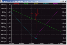
LTspice simulations are attached. The attached 'Ic-gm-zero-crossing-15W-50Hz' png shows the zero crossing current and crossover gain wobble which is quite large and very sharp with lots of high order harmonics.
The Faran THD at 15W (max power 20W) is 0.04% which seems quite low compared to de Jager's amp. But we need to weight the high order harmonics to compare the Falks distortion 'sound' to other amps, like de Jager and my CSD. The 'Faran-CSD-sims' zip has a circuit that performs weighted distortion. It gives a weighted THD (wTHD) of 10% at 15W - that's a massive factor of 250 times the unweighted THD.
The “minimal cross-over distortion” of 0.04% at full power is misleading, because when it is weighted, it is more like 10% at full power. And the weighted distortion goes higher at 1W. A good example of why unweighted THD is a meaningless figure unless the harmonic structure is also quantified. It can be quantified using weighting filters (which can be used for bench testing as well as simulations) or it can be done by noting the average roll-off slope of the higher harmonics (needs to be faster than -40dB/decade). The weighting filter approach is covered in Linear Audio Vol.4 and the harmonic roll-off is covered in my Cube amp Supplement on myDrive (link in Sig line).
I'll post the de Jager wTHD sim in a following post. It gives 0.04% unweighted THD at 30W and 0.1% wTHD, a factor of about 2 when weighted, which indicates negligible high order distortion and highlighting the advantage of the de Jager biasing loop. The Linear Audio CSD amp gives a factor of 4 when weighting distortion showing it also has mainly low order distortion.
BTW for the Faran simulation I have used the same transistors as the de Jager amp for comparison. I tweaked the feedback capacitor for stability. I increased the original Cr of 10uF to 100uF for less phase shift at 50Hz (for better FFT's).The driver and power transistor beta's have been matched. You can mismatch them to see how much distortion it creates.
You can see the Faran current source driven OPS is a simple circuit and has excellent thermal stability (set Temp=177C for the power transistors and drivers).
To check if the Faran amp distortion is audible I have another post following with a Faran simulation using a 'wav' file of a guitar strum and the amp output is recorded to a 'wav' for replay and listener comparison. It's a seldom used feature of LTspice but may be limited by a 16 bit word.
My PC is not suitable quality to hear the difference with the Faran amp simulation.
Please do a listener test to see if the Faran amp distortion is audible on your system. You can PM me.
Attachments
de Jager weighted THD sim
Hi Tibouchina,
The de Jager wTHD sim is attached.
As mentioned it gives 0.04% unweighted THD at 30W and 0.1% wTHD, a factor of about 2 when weighted, which indicates negligible high order distortion and highlighting the advantage of the de Jager biasing loop. The Linear Audio CSD amp gives a factor of 4 when weighting distortion showing it also has mainly low order distortion.
If this stuff is new to others, the THD and wTHD values are read in the ErrorLog (Ctrl+L). The first 300 harmonics are used in these weighted sims to cover up to 15kHz. And 50Hz is used because that is the most sensitive hearing test so the high order harmonics fall in the sensitive hearing range of 300Hz to 3kHz band. For more on the weighting filter approach see my article in Linear Audio Vol.4. Rather than add weighting filters to all your simulations and bench tests you can get a good estimate from the rate the harmonics roll-off. This idea is not in my article, it is a more recent idea that is covered in my Cube amp Supplement (IansDrive link in Sig line).
BTW This is the modified de Jager circuit I posted previously with small signal transistors for Q6,7,8 and added a 'keep-on' resistor. I increased Cr to 470uF and shorted the input capacitor for less phase shift at 50Hz for better FFT's.
Attachments
Last edited:
My simulation of Faran amplifier was not so good.
The design is certainly in the spirit of this thread and maybe the design can be improved without adding too much complexity. There are also some other interesting topologies mentioned in the paper.
This amplifier was originally implemented using germanium devices. The output is pure class B. The results of my simplistic simulation of the output stage with power transistors gave harmonic distortion approaching 10% (no feedback). Odd order harmonics were prevalent. The problem mainly due to a slow transistor turn on after been subjected to a large reverse Vbe voltage.Hi Tibouchina,
LTspice simulations are attached. The attached 'Ic-gm-zero-crossing-15W-50Hz' png shows the zero crossing current and crossover gain wobble which is quite large and very sharp with lots of high order harmonics.
The design is certainly in the spirit of this thread and maybe the design can be improved without adding too much complexity. There are also some other interesting topologies mentioned in the paper.
Faran distortion simulations using a 'wav' file
Hi Tibouchina,
The de Jager 'wav' sim is attached.
As mentioned it is a nifty way to check if the Faran amp distortion is audible. The 'wav' input file is a 'clean' guitar strum. The amp output is recorded to a 'wav' for replay and listener comparison. The output wave level has bee set for playback to within 1dB of the input wave level for a direct A/B comparison. You can add your own input signal using a wave editor. I used Audacity which is free open source.
There is also a second sim file for a fixed tone, presently set to middle C. It records the input and output waves at the same time for a direct A/B comparison.
Attachments
Last edited:
Faran's may be useable in Lo-Fi apps with modern BJT's
My sims use much faster modern transistors. Listening to the generated wave files (at least on my Low-Fi PC speakers and amp) there does not appear to be lots of distortion, unlike the original germanium amplifier.
So maybe Faran's simple topology (Fig.5) and freedom from thermal biasing problems is usable in some applications where super-Hi-Fi isn't needed. Maybe for a guitar amp?
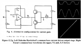
You mention Faran's other ideas in his paper. I think Paul Mills and Malcolm Hawsksford used the Faran's common-base arrangement in their Transconductance amp JAES October 1986, eg, Fig. 4, see attached.
...The design is certainly in the spirit of this thread and maybe the design can be improved without adding too much complexity. There are also some other interesting topologies mentioned in the paper.
My sims use much faster modern transistors. Listening to the generated wave files (at least on my Low-Fi PC speakers and amp) there does not appear to be lots of distortion, unlike the original germanium amplifier.
So maybe Faran's simple topology (Fig.5) and freedom from thermal biasing problems is usable in some applications where super-Hi-Fi isn't needed. Maybe for a guitar amp?
You mention Faran's other ideas in his paper. I think Paul Mills and Malcolm Hawsksford used the Faran's common-base arrangement in their Transconductance amp JAES October 1986, eg, Fig. 4, see attached.
Attachments
A simplisitc evaluation of the Faran amp.
It is optimistic to image that a class B output with common bases will generate good quality audio. But as you mentioned it is acceptable for other applications. In the early 1960's this amplifier would have been an ideal solution (maybe) for radiograms, record players and maybe even a low powered PA system. The published distortion specification sounds slightly implausible. The thing that struck me about the paper was the quality of the presentation and formatting. Faran had previously done some very good work in acoustic scattering.
I evaluated the design by just looking at the output stage driven by a current source. The simulation files are attached. The plot of the current through the load (Iload.png) illustrates crossover distortion. To illustrate the base charge draining refer to the plot of the base currents (BaseCurrents.png). This shows a reverse base current while charge is drained from the device. The reverse current causes the other output device to be starved of base current, delaying the supply of current to the load. This amplifier design is not the solution. The only way forward is to split the common base connection and drive the devices from two current sources.


Ian, Thanks for the simulations and sound files. I will digest these tonight.So maybe Faran's simple topology (Fig.5) and freedom from thermal biasing problems is usable in some applications where super-Hi-Fi isn't needed. Maybe for a guitar amp?
It is optimistic to image that a class B output with common bases will generate good quality audio. But as you mentioned it is acceptable for other applications. In the early 1960's this amplifier would have been an ideal solution (maybe) for radiograms, record players and maybe even a low powered PA system. The published distortion specification sounds slightly implausible. The thing that struck me about the paper was the quality of the presentation and formatting. Faran had previously done some very good work in acoustic scattering.
I evaluated the design by just looking at the output stage driven by a current source. The simulation files are attached. The plot of the current through the load (Iload.png) illustrates crossover distortion. To illustrate the base charge draining refer to the plot of the base currents (BaseCurrents.png). This shows a reverse base current while charge is drained from the device. The reverse current causes the other output device to be starved of base current, delaying the supply of current to the load. This amplifier design is not the solution. The only way forward is to split the common base connection and drive the devices from two current sources.
Attachments
Last edited:
A simple modification to reduce cross-over effects.
A simple way to prevent the reverse base current is to use a blocking diode as shown in the revised schematic. The base currents no longer have the reverse current spike as shown in the plot below. The cross over distortion in the output current is reduced, but not eliminated
This shows a reverse base current while charge is drained from the device. The reverse current causes the other output device to be starved of base current, delaying the supply of current to the load.
A simple way to prevent the reverse base current is to use a blocking diode as shown in the revised schematic. The base currents no longer have the reverse current spike as shown in the plot below. The cross over distortion in the output current is reduced, but not eliminated
Attachments
A simple way to prevent the reverse base current is to use a blocking diode as shown in the revised schematic. The base currents no longer have the reverse current spike as shown in the plot below. The cross over distortion in the output current is reduced, but not eliminated
Interesting idea. Adding blocking diodes halves the weighted THD at 50Hz. But no improvement with unweighted THD (another reminder that THD is meaningless).
But the blocking diodes prevent charge pull-out. Now you can't run the amp continuously much above 20kHz due to cross-conduction dissipation. The original circuit without the blocking diodes can run to 200kHz with only a few mA of cross-conduction. Amazing!😎
In the attached zip I have 3 simulations. The one with blocking diodes added is in"...mod1" and it gives 0.5% wTHD at 50Hz and 15W (near full power), down from 10%. Most of this reduction is from adding faster drivers (2N3904/6) which are about 10 times faster than the original drivers (BD139/140).
To see the effect of just faster drivers see the "...mod" file which reduces the wTHD to 1%. See the attached Ic and Vout capture. Notice the reverse emitter current through Tr12 does not distort the Vout waveform, presumably because the reverse current flows through the load. So I don't see much advantage adding the blocking diodes. Far better to use very fast driver transistors. At 1W 50Hz the wTHD is 4%. Unweighted 50Hz is 0.01%, and 0.1% at 1kHz and 1% at 20kHz.
So with the faster drivers and no blocking diodes, the unweighted distortion figures are almost 'transparent' even at 1W (by 'transparent' I mean harmonics are below the hearing threshold when masking is taken into account). And faster drivers brings the unweighed THD vs frequency close to the original de Jager amp -- but with immunity from cross-conduction dissipation.
So the simpler version without blocking diodes definitely has potential for Med-Fi apps like guitar amps. There may be some mods that could get the wTHD lower. Any suggestions? Also mods for standard dual-rail operation.
A battery powered amp needs mods for single supply operation. This topology is the closest to true Class-B that I have seen; where 99% the idle current goes into the the pre-drivers (6mA) plus the input stage (another 6mA) - virtually zero idle current into the drivers and power transistors.
The third sim in the attached zip has the blocking diodes and charge pull-out transistors to short the base to emitters (so no charge flows via the load). The weighted THD is halved (compared to just faster drivers). It can now run to 200kHz with only a few mA of cross-conduction. But if you are after simplicity for a Med-Fi amp then the added parts are not worthwhile IMO.
Attachments
Listening to amps in simulation is actually quite interesting, and you can even run a stereo pair together.
You might get some ideas here 🙂
http://www.diyaudio.com/forums/lounge/303727-welcome-virtual-listening-room.html
You might get some ideas here 🙂
http://www.diyaudio.com/forums/lounge/303727-welcome-virtual-listening-room.html
Cross-Conduction Dissipation
At 20 kHz the cross-conduction currents are small and are self-quenching. My concern is that they contribute to non-linear behavior of the output stage.
But the blocking diodes prevent charge pull-out. Now you can't run the amp continuously much above 20kHz due to cross-conduction dissipation. The original circuit without the blocking diodes can run to 200kHz with only a few mA of cross-conduction. Amazing!😎
At 20 kHz the cross-conduction currents are small and are self-quenching. My concern is that they contribute to non-linear behavior of the output stage.
- Status
- Not open for further replies.
- Home
- Amplifiers
- Solid State
- Current-Source-Driven-power-transistors-and-mitigating-cross-conduction-distortion