You get two resistors 310 and 80 ohms. But I'm not sure that the circuit will work correctly.
The power of the amplifier will probably decrease.
The power of the amplifier will probably decrease.
Last edited:
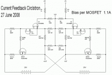
Idle Power Consumtion
Hi,
just a short question about this circlotron:
How much idle current per output device is necessary for this amp?
Hi,
just a short question about this circlotron:
How much idle current per output device is necessary for this amp?
Hi,
just a short question about this circlotron:
How much idle current per output device is necessary for this amp?
The answer is in message #76 and #77.
300mA, so a Circlotron needs more idle current than a "normal" Class AB amp.The answer is in message #76 and #77.
Hi,
What have to modify when I like rather to use lateral MOSFET instead of IRFP trans. I thought 2SK1058/ECW10N20-S/ECW20N20-S types but their Vgs parameters lower.
If I good understand the value of Mosfet Vgs come from the R12-392ohm and I12 is 10,03mA. So Vgs=392*0,0103=3,9V. In the simulation the Id bias of IRFP150n is 300mA, If I want same bias Id of lateral MOSFET's, the Vgs=0,8V Id=200mA of 2SK1058 and the I12 same 10,03mA so new R12=80ohm (0,8/0,01). I this case bias of ECW20N20 would be Id=400mA. Is it correct?
Gate resistors (100-300 ohm) before M1/M2 not necessary?
Gy.
Hi, why do you want using lateral mosfet ?
in simulation the distortion increases enormously with the exicon, very low transconductance
I have 4 ECW20N20-S and long tried to use them to benefit from their thermal stability, but here it is useless.
It could be, but lot of audio company use these instead of cheapest IRF series.Hi, why do you want using lateral mosfet ?
in simulation the distortion increases enormously with the exicon, very low transconductance
I have 4 ECW20N20-S and long tried to use them to benefit from their thermal stability, but here it is useless.
They are more linear, internal capacitance are smaller than HEXFETs, so may have a small improvement in performance.
I build 20 years ago an AB class amp with IRF540/IRF9540 pair and was big disappointment. The situation is not same of course but I lost my trust in hexfet.
You are in easy situation, you have 4 pieces (-S selected!) you can check whats the truth in this case.
Last edited:
I have several IR vs-fa57sa50lc, which is a MOSFET module. I want to increase the power supply to 50V or 75V, but j113 can only withstand 35V voltage. What JFET can I replace? I use translation software, hope you can understand.
out of my knowledge... good sounding jfet in that voltage range doesnt exist.
you can try making a cascode on top of them.
but that would require an exstensive round of simulations to see how all the other factors will need to adjust against the the mod.
maybe ultimate can help you better than me
you can try making a cascode on top of them.
but that would require an exstensive round of simulations to see how all the other factors will need to adjust against the the mod.
maybe ultimate can help you better than me
I want to increase the power supply to 50V or 75V, but j113 can only withstand 35V voltage.
You can cascode the J113s with higher voltage BJTs for more power. I can't post a diagram right now, but will follow up with one later.
I just went to mouser to see it, but I didn't. If I can't raise the voltage, can I use 2sk170 instead?
I have PSPICE for fa57sa50.
.SUBCKT fa57sa50lc 1 2 3
**************************************
* Model Generated by MODPEX *
*Copyright(c) Symmetry Design Systems*
* All Rights Reserved *
* UNPUBLISHED LICENSED SOFTWARE *
* Contains Proprietary Information *
* Which is The Property of *
* SYMMETRY OR ITS LICENSORS *
*Commercial Use or Resale Restricted *
* by Symmetry License Agreement *
**************************************
* Model generated on Dec 14, 01
* MODEL FORMAT: SPICE3
* Symmetry POWER MOS Model (Version 1.0)
* External Node Designations
* Node 1 -> Drain
* Node 2 -> Gate
* Node 3 -> Source
M1 9 7 8 8 MM L=100u W=100u
.MODEL MM NMOS LEVEL=1 IS=1e-32
+VTO=3.85566 LAMBDA=0.0153185 KP=14.024
+CGSO=9.662e-05 CGDO=8.7e-12
RS 8 3 0.0001
D1 3 1 MD
.MODEL MD D IS=1.06902e-16 RS=0.00795354 N=0.643552 BV=500
+IBV=0.00025 EG=1 XTI=1 TT=0
+CJO=7.9e-09 VJ=3.64448 M=0.9 FC=0.5
RDS 3 1 1e+06
RD 9 1 0.06
RG 2 7 6
D2 4 5 MD1
* Default values used in MD1:
* RS=0 EG=1.11 XTI=3.0 TT=0
* BV=infinite IBV=1mA
.MODEL MD1 D IS=1e-32 N=50
+CJO=8.86563e-09 VJ=0.5 M=0.9 FC=1e-08
D3 0 5 MD2
* Default values used in MD2:
* EG=1.11 XTI=3.0 TT=0 CJO=0
* BV=infinite IBV=1mA
.MODEL MD2 D IS=1e-10 N=0.400063 RS=3e-06
RL 5 10 1
FI2 7 9 VFI2 -1
VFI2 4 0 0
EV16 10 0 9 7 1
CAP 11 10 8.86563e-09
FI1 7 9 VFI1 -1
VFI1 11 6 0
RCAP 6 10 1
D4 0 6 MD3
* Default values used in MD3:
* EG=1.11 XTI=3.0 TT=0 CJO=0
* RS=0 BV=infinite IBV=1mA
.MODEL MD3 D IS=1e-10 N=0.400063
.ENDS fa57sa50lc
Floating Cascode
This conceptual diagram shows one approach to cascoding the input stage. There are other ways to do essentially the same thing, but I think this one shows the idea clearly.
Recall that the feedback network consists of two 1K resistors feeding signal current through a 100 ohm resistor, creating a feedback voltage across the input JFET sources that is 1/20 of the output voltage. We want the cascode to replicate that signal voltage across the drains of the input JFETs at a DC level that gives the JFETs good operating room while staying well below their maximum Vds limits.
To accomplish this we use a second resistor network giving the same feedback ratio as the first, here consisting of two 22.1K resistors feeding signal current through a 2.21K resistor. This creates a feedback signal voltage across the cascode BJT bases and thus also (minus one Vbe) across the input JFET drains. The DC level of the cascode voltage is set by two zener shunts (I used 15V), each tied across one floating power supply and referenced to the output lines.
This arrangement results in a signal voltage across the drains of the input JFETs that closely tracks the voltage across their sources. With balanced input signals, this holds the Vds of each JFET nearly constant at slightly less than the zener voltage. For unbalanced input signals, it causes the input JFETs to experience relatively small Vds variations roughly equal to the input signal voltage.
Attachments
This conceptual diagram shows one approach to cascoding the input stage. There are other ways to do essentially the same thing, but I think this one shows the idea clearly.
Recall that the feedback network consists of two 1K resistors feeding signal current through a 100 ohm resistor, creating a feedback voltage across the input JFET sources that is 1/20 of the output voltage. We want the cascode to replicate that signal voltage across the drains of the input JFETs at a DC level that gives the JFETs good operating room while staying well below their maximum Vds limits.
To accomplish this we use a second resistor network giving the same feedback ratio as the first, here consisting of two 22.1K resistors feeding signal current through a 2.21K resistor. This creates a feedback signal voltage across the cascode BJT bases and thus also (minus one Vbe) across the input JFET drains. The DC level of the cascode voltage is set by two zener shunts (I used 15V), each tied across one floating power supply and referenced to the output lines.
This arrangement results in a signal voltage across the drains of the input JFETs that closely tracks the voltage across their sources. With balanced input signals, this holds the Vds of each JFET nearly constant at slightly less than the zener voltage. For unbalanced input signals, it causes the input JFETs to experience relatively small Vds variations roughly equal to the input signal voltage.
Thank You!
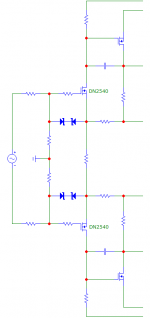
I tried to replace j113 directly with dn2540, and the simulation test was successful. Dn2540 withstand voltage is 400V, can I change it like this? What else needs to be improved? The following is the PSPICE code for dn2540:
*DN2540 MODEL
*
.MODEL DN2540 NMOS (LEVEL=3 RS=1.05 NSUB=5.0E14
+DELTA=0.1 KAPPA=0.20 TPG=1 CGDO=3.1716E-10
+RD=11 VTO=-1.50 VMAX=1.0E7 ETA=0.0223089
+NFS=6.6E10 TOX=725E-10 LD=1.698E-9 UO=862.425
+XJ=6.4666E-7 THETA=1.0E-5 CGSO=2.50E-9 L=4.0E-6
+W=59E-3)
Dn2540 withstand voltage is 400V, can I change it like this? What else needs to be improved?
With DN2540s you won't need cascodes, but with +/- 20V maximum Vgs, you may want to add zener clamps at the input(s) for protection.
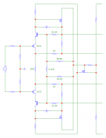
In case it's needed, here's a diagram to clarify my earlier comment about zener clamps. I've also added a resistor to isolate each DN2540 gate from the low impedance of the zeners if they go into conduction, as this has been known to cause oscillation.
Also shown is a second method of cascoding a J113 input stage. Same basic principle as before, but instead of zener shunts to set the cascode DC level, this method uses two 39.2K resistors to form voltage dividers with the two 22.1K resistors, pulling up both BJT base voltages.
Micro-Cap 12 comes with models for both J113 and DN2540 devices, so I compared their performance as shown in these two circuit diagrams. I see similar frequency response but lower distortion with the DN2540, perhaps due to its much greater transconductance. Worth a try at least...
Attachments
Last edited:
In case it's needed, here's a diagram to clarify my earlier comment about zener clamps. I've also added a resistor to isolate each DN2540 gate from the low impedance of the zeners if they go into conduction, as this has been known to cause oscillation.
Also shown is a second method of cascoding a J113 input stage. Same basic principle as before, but instead of zener shunts to set the cascode DC level, this method uses two 39.2K resistors to form voltage dividers with the two 22.1K resistors, pulling up both BJT base voltages.
Micro-Cap 12 comes with models for both J113 and DN2540 devices, so I compared their performance as shown in these two circuit diagrams. I see similar frequency response but lower distortion with the DN2540, perhaps due to its much greater transconductance. Worth a try at least...
How efficient you are! The simulation results are so fast. Do I see another MOSFET's direction reversed? Also, please post all the circuit diagrams of dn2540, thank you.
Yes, unfortunately the arrows in the PMOS symbols do not point away from the gate, but that is how it appears in the model (OnSemi FQP3P20).
The remainder of the test circuit appears as shown in post #215. However, we are now talking about an amplifier with 50+ volt rails. In real life, an output stage with multiple MOSFET pairs and source resistors may be needed for best reliability.
The remainder of the test circuit appears as shown in post #215. However, we are now talking about an amplifier with 50+ volt rails. In real life, an output stage with multiple MOSFET pairs and source resistors may be needed for best reliability.
- Home
- Amplifiers
- Solid State
- Current feedback Mosfet Circlotron