Small correction above; other VFA compensation types may have intrinsic high slew rates (notably the input inclusive compensation) although this may come at the price of less flexibility in applications, making them potentially undesirable for ICs.
That is absolutely correct.
Hans, that's because the circuit under test has those components. The only thing Middlebrook adds is Vtest and Itest.
It would really help me out if you posted the .asc file with the Middlebrook equations.
It would really help me out if you posted the .asc file with the Middlebrook equations.
Arf.I'm more than willing to try this after I already tried with the LT1395.
Send me a CFA of your own and I will show the results.
Don't you see all the differences between a *discreet* POWER AMP with FET in the output stage and a BJT IC ?
I will NEVER even try to put such a cap on any CFA IC, and I used thousands during decades. This little cap is not used to stabilize the amp (stupid), and has no or very little effect on its bandwidth/phase margin. Just used to optimize "litle signals" in this particular topology I indicated.
You can understand your "believes" do not interest-me so much as they do not have much weight in front of my real life experience with real parts (i design CFAs amps since more than 30 years).
Feel free to try-it or not, it is YOUR problem. And it will be my last words on this subject.
Why don't you try at least to simulate it ?
I have several CFA (laterals power fets) perfectly stable tuned this way.
I’ve spent hours on the simulator looking into this re CFA and VFA. Generally, I don’t use this on my VFA designs and never on a CFA.
OK.
I'm afraid I don't entirely understand what you are saying. I do believe that a comparison of the impedances looking in both directions at in (-) will establish what DIT will: the predominant form of feedback in the circuit.
Could you please explain further the point you are making above?
Loop feedback begins with an initial stimulus entering the system, that in the feedback loop ends with counter-signalling that suppresses the original stimulus (mentioned previously as a shunting action). The initial stimulus is represented by the top Figure as attached, whereupon the Tz node resistor Rz is shorted to ground.
In the determination of the propriety of a particular CFA device being so described and connected in a specific network doesn't require feedback. The middle figure is an equivalent circuit that contains the resistances on either side of Vo1.
It is considered that when the value of resistance on the left of Vo1 is equal to the equivalent resistance on the right of Vo1 there is no dominant source, either by the battery or by the input buffer feeding through Ro at Vo1. Bear in mind that feedback isn't released, hence one side is indifferent from the other in terms of dominance and that initial stimulus can be applied at the input to the input buffer or at the opposing end by a variant battery voltage.
As Ro1 diminishes to zero, voltage dominance occurs at the inverting terminal. This means that the inverting terminal can source theoretically infinite current to any output load connected to it. This has the effect that the inverting terminal as a voltage source is entirely current controlled by the resistance in series with its output as the only path it can source current.
The bottom figure can be ignored.
Attachments
Loop feedback begins with an initial stimulus entering the system, that in the feedback loop ends with counter-signalling that suppresses the original stimulus (mentioned previously as a shunting action)...
Hierfi, before we discuss, I do hope to pursue my discussion with forr. I don't want to create a diversion. I hope you understand.
Chris,
look at the Middlebrook layouts below.
The certainly have an Rf and a Rg.
But send me what you want to see for Rf and Rg and I'll do a sim for you.
Hans
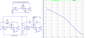
Hans, here's how Middlebrook's DIT should be applied to the circuit I posted. The circuit's input signal is zeroed. In one case, the loop is broken to insert a voltage source; in another, a current is inserted at the point where the loop was broken with the voltage source. The ratios of the reverse to the forward signal can be calculated. No other circuit components are to be added, because that would modify the circuit to be analyzed.
In the attachment, V(vf) is essentially zero. I had to add a very small number (1E-8) to it so I could display a ratio.
The voltage loop gain is essentially infinite, while the current loop gain is finite. It is clear that here, current feedback predominates.
Attachments
Chris,
look at the Middlebrook layouts below.
The certainly have an Rf and a Rg.
But send me what you want to see for Rf and Rg and I'll do a sim for you.
Hans
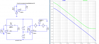
Next I went back to the circuit in which I had thought that c.f. predominated, but which your tests led me to believe I was wrong. I guess I didn't realize how you were running your tests, because the attached shows that indeed, c.f. predominates.
Attachments
I Just want to add I use this this little cap here (in // with the serial feedback resistance witch, I agree, seems strange in a CFA) to work only around the pole created by the serial feedback resistance and the parasitic capacitance in the emitter of the input transistor.And it will be my last words on this subject.
It need to be carefully sized on the bench as it depend on the parasitic capacitances of the wiring too. If you increase its value, it will lead, indeed, to instability.*
Using Diamond inputs stage (Highly recommended), a good thing is to add a RC low pass filter at the base of the second transistors of the diamond. It will protect the amp from any TIM, be independent from the source impedance and will prevent overshoot of little signals as well. Diamonds are prone to be instable at very high frequencies.
* 10pF with 1KOhm has a FC of 16MHz.
I take great care of the quality of this serial resistance. No inductive and oversized for dissipation. Often, I use 2 // Dale, here.
Too, the output signal that goes in this resistance has to be taken directly at the output pin (or the point that enter in your output protecting coil if you use one) with nothing else connected in between apart your miller caps.
Just my two cents.
Last edited:
Tournesol,
This is not an unimportant aspect. The answer would be a resounding no. Transistors have insufficient ability to cope with the wide signal spectrum even at fairly low level amplification and light loads. Most amplifiers exhibit poor bandwidth therefore massive high frequency distortion. Obtaining good high frequency response is a cumbersome balancing act and as far as I can tell, the subject has been entirely left out of the scope of discussion on this website. High frequency response is the main distinguishing quality factor between amplifiers.
The need for compensation capacitor is an unmistakable sign of sickness, such as the presence of malicious phase relationships and severe instability not just at high frequencies but at all frequencies. The compensation capacitor further shrinks the already pitiable bandwidth.
Are actual solid state devices fast enough to provide flat open loop at 20KHz in a high gain power amp ?
This is not an unimportant aspect. The answer would be a resounding no. Transistors have insufficient ability to cope with the wide signal spectrum even at fairly low level amplification and light loads. Most amplifiers exhibit poor bandwidth therefore massive high frequency distortion. Obtaining good high frequency response is a cumbersome balancing act and as far as I can tell, the subject has been entirely left out of the scope of discussion on this website. High frequency response is the main distinguishing quality factor between amplifiers.
The need for compensation capacitor is an unmistakable sign of sickness, such as the presence of malicious phase relationships and severe instability not just at high frequencies but at all frequencies. The compensation capacitor further shrinks the already pitiable bandwidth.
Sorry Chris,Hans, here's how Middlebrook's DIT should be applied to the circuit I posted. The circuit's input signal is zeroed. In one case, the loop is broken to insert a voltage source; in another, a current is inserted at the point where the loop was broken with the voltage source. The ratios of the reverse to the forward signal can be calculated. No other circuit components are to be added, because that would modify the circuit to be analyzed.
In the attachment, V(vf) is essentially zero. I had to add a very small number (1E-8) to it so I could display a ratio.
The voltage loop gain is essentially infinite, while the current loop gain is finite. It is clear that here, current feedback predominates.
To my opinion you are quite misinterpreting the Middelbrook DIT.
A circuit to be analysed with a DIT should have three handles, a positive and a negative input plus an output.
You have created some Alien with 4 handles. First three being the positive and the negative input plus output all directly from the LT1001.
But a fourth handle is created by using the output of the current source, in your schematic G1 and G2.
When applying a DIT, either the output of the LT1001 or the output of the current source should be serving the role as being the output.
Apart from that, you have changed the original 100K//10pF into 10K//100pF.
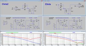
I made two new sims, but now both with circuits with the correct amount of 3 handles.
One with the output from the LT1001 as before, the other one with the current source as the output.
And I also changed to 10K//100pF and used a very large value of 1 Gig for Rg, because without Rg, Vr/Vf went through the roof and with a value of 100Meg and lower, the circuit already turns from a CFA into a VFA.
The value of Rf is left as before at 500 Ohm, changing this to lower values, didn't change anything.
To conclude: with a DIT test with Rg>1Gig, the one with "Chris" turned out as a VFA and the one with "Chris2" as a CFA.
With Rg<100Meg both are VFA's.
Hans
Attachments
Well, that would be great news. According to this the LT1001 turns out to be a CFA !Next I went back to the circuit in which I had thought that c.f. predominated, but which your tests led me to believe I was wrong. I guess I didn't realize how you were running your tests, because the attached shows that indeed, c.f. predominates.
In both cases you have connected the upper side of the 100 Ohm resistor to the minus input of the LT1001, instead of to the upper side of R4.
Changing that will give you the Middlebrook test and show that a LT1001 is a pure VFA.
Hans
Middelbrook DIT.
Middelbrook DIT.
Links about this author and his DIT would be helpful.
Thanks in advance.
Middelbrook DIT.
Links about this author and his DIT would be helpful.
Thanks in advance.
This is not an unimportant aspect. The answer would be a resounding no. Transistors have insufficient ability to cope with the wide signal spectrum even at fairly low level amplification and light loads.
This is of of course nonsense. Even here there are open-loop amps with 90+dB THD into 1K loads with 250kHz plus BW.
N101N writes remarkably similarly to Moo Koo and seems to harbour the same electrical fantasies.
I Just want to add I use this this little cap here (in // with the serial feedback resistance witch, I agree, seems strange in a CFA) to work only around the pole created by the serial feedback resistance and the parasitic capacitance in the emitter of the input transistor.
It need to be carefully sized on the bench as it depend on the parasitic capacitances of the wiring too. If you increase its value, it will lead, indeed, to instability.*
This may be something you haven't considered. The feedback network can be likened to a 10x oscilloscope probe. The Rf resistor and Rg resistors each have controlled capacitances across them, that when the time constants of each resistor in parallel with its associated capacitance is equal, a square wave results at the point of division. The square wave is trimmed with a variable capacitor. Notwithstanding that this can still lead to oscillations it is something to consider in your design. Circuit layout and design always creates some form of parasitic capacitance across the Rg resistor.
* 10pF with 1KOhm has a FC of 16MHz.
I take great care of the quality of this serial resistance. No inductive and oversized for dissipation. Often, I use 2 // Dale, here.
This is valid reasoning. Feedback resistors are outside the feedback loop as part of the reference network. This is also why the quality of the input buffer must be the highest quality as opposed to the output buffer which can be rubbish, as it falls inside the feedback loop.
N101N writes remarkably similarly to Moo Koo and seems to harbour the same electrical fantasies.
Nah, more like a touch of KBK.
Sorry Chris,
To my opinion you are quite misinterpreting the Middelbrook DIT.
Hans
Right back at you, Hans! Let's congratulate ourselves on what appears to be a legitimate disagreement and not a misunderstanding.
My understanding of Middlebrook's DIT is as follows:
A given circuit is normally used with a signal source to excite it. We leave the source connected but set it to zero.
We choose where in the circuit we want to test loop gains: node X. For us, this will be the inverting input.
The first test is to break the loop at X and insert a voltage source to close the break. We can measure the forward and reverse voltages and take the ratio of the latter to the former.
The second test is to connect a ground-referenced current source to point X. We can measure the forward and reverse currents and take the ratio of the latter to the former.
The lesser of the two gains is associated with the more (predominant form of) feedback.
Please consider Sergio Franco's excellent article that covers this topic at https://www.edn.com/design/analog/4458753/1/In-defense-of-the-current-feedback-amplifier . In Figure 6, he shows how to test the closed loop voltage gain of a particular CFA. No surprises here - this isn't Middlebrook.
In Figure 11, he shows how to examine the types of feedback at the summing node of that very same circuit. Please take note - other than the voltage source that closes the break, and the current source added (plus the 0V sources so he has something to measure the current through) no components were added to or removed from the circuit under test. To have done so would have been to have tested a different circuit from the one whose closed loop voltage gain was tested.
Perhaps I have not convinced you. If so, can you and I dig deep into this article to find the root source of our disagreement?
- Home
- Amplifiers
- Solid State
- Current Feedback Amplifiers, not only a semantic problem?