No I did not
Sorry but you are wrong, I used the whole thing including everything.
Please have another look at the circuit that I used below.
When I connected something wrong, tell me.
Hans
Please show me the complete circuit without subcircuits obscuring the view and apply DIT to it. Thanks in advance.
My oh my, this is quite a debate raging here; I don't really understand what's the contention, though. One thing I can tell (from my past work with CFAs) is that no new feedback topology (beyond the four known) is required to explain each and every aspect of the CFA small signal properties. Each and every CFA property can be explained within the existing mathematical formalism, for the shunt output, serial input feedback topology. Of course, the textbook CFA analysis approach (based on current summing at the inverting input) is much simpler, but then again, it does not define a new "feedback type", at least because that analysis is not a formalism that can be extended to an abstract model, based on the standard black box two-port networks. I'll try to find my old notes and post a summary in PDF (since the algebra is non trivial). If I recall correctly, the CFA is exactly equivalent to a voltage-sampling series-mixing (series-shunt) topology (also known as a "voltage feedback") but with the observation that in the range of closed loop gains where the CFA small signal properties are important, the open loop gain depends on the feedback network (which is never happening in an amplifier commonly known as a VFA, where the open loop gain is only a function of the amplifier two-port network).
As of the large signal behavior (notably the much praised high slew rate) I don't believe it is specific to the CFA concept; it is IMO a property of a particular circuit topology implementing a CFA. I'm not sure if another CFA circuit topology (beyond the common base inverting input) exists... To have the same slew rate performance, a classic VFA would have to either run a very hot input stage, use rather high value capacitors to dump current in the compensation network (see the Stochino amp) or to use the H bridge topology. Of course, only the last is a real option for an IC modern implementation.
As of the large signal behavior (notably the much praised high slew rate) I don't believe it is specific to the CFA concept; it is IMO a property of a particular circuit topology implementing a CFA. I'm not sure if another CFA circuit topology (beyond the common base inverting input) exists... To have the same slew rate performance, a classic VFA would have to either run a very hot input stage, use rather high value capacitors to dump current in the compensation network (see the Stochino amp) or to use the H bridge topology. Of course, only the last is a real option for an IC modern implementation.
Chris,Please show me the complete circuit without subcircuits obscuring the view and apply DIT to it. Thanks in advance.
We really have a small problem ha, ha, but nothing seriously that can't be solved.
I'll do my best trying again to explain how LTSpice works.
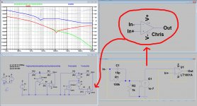
Look at the image below.
I made a subckt and called it Chris.asc, being your design in completeness as shown in the image below at the right bottom with 5 so called Ports resp: In+, In-, V+, V- and Out.
With an Chris.asy file I made the reference to this whole subckt look just like an op amp when being inserted, again with In+, In-, V+, V- and Out.
So when calling "Chris" it looks just like any op amp, but in this case your complete subckt is inside.
This makes it much easier to insert "Chris" in my DIT test circuit, below left, where the circuits to be tested should have this op amp shape.
Now when doing a DIT with "Chris", all I have to do is to insert this self created component that looks like an op amp, but which it is not, in my DIT test model.
I hope this makes it clear what I did, and takes away your doubts that I did not use your complete circuit.
Hans
Attachments
Please excuse my intervention in your ongoing dialog. I have attached a diagram that I believe is less confusing of what you may be, at least in part, trying to convey.
I moved your Vin from the control and feedback loop in order to convey that it is in isolation as largely irrelevant from what I consider is the core of the discussion. I added Rx as the Tz node resistance and Rl as an external load resistance. It is considered that the direction of current flow as always output from the current mirrors into Rx (however that came to pass), dictates the output current polarity from the output of the inverting terminal, Rg and Rl. Currents in Rf reverses as dependent on voltage gain around unity.
Figure 2 indicates that the Amp output buffer sinks current into itself as sourced by the inverting terminal. This indicates that current reversal only occurs in the output buffer. CFA's works on the principle of shunting current away from inverting terminal current, not by feeding current into it.
I consider that considerable confusion exists by failing to identify the input network as a "current sensing output buffer". Although this might suggest some form of voltage feedback amplifier this isn't considered true.
Attachments
Please excuse my intervention in your ongoing dialog.
Hierfi, forr, I'm sorry, but this has confused me and raised too many questions. Please allow forr and me to finish our discussions.
Regards, CPaul
Hierfi, forr, I'm sorry, but this has confused me and raised too many questions. Please allow forr and me to finish our discussions.
Regards, CPaul
Sure
select Chris to insert him in your schematic.
Hans
I think that is against forum rules

Jan
And here are Chris.asc and Chris.asy in a zip file.
Unzip them, put them in your LTSpice directory and use them by clicking on TOP DIRECTORY and select Chris to insert him in your schematic.
Hans
Post 1668 adds resistor R2 that is not in the circuit I posted. With R2 added, the impedance of the feedback network is a lot lower than that of the inverting input, so of course the circuit will have predominantly v.f.
You've built a nice .asc with the equation embedded in it to perform DIT. I could insert my own circuits into the file and perform DIT on them. Would you be so kind as to post it? Thanks in Advance.
To have the same slew rate performance, a classic Miller compensated VFA would have to either run a very hot input stage, use rather high value capacitors to dump current in the compensation network (see the Stochino amp) or to use the H bridge topology.
Small correction above; other VFA compensation types may have intrinsic high slew rates (notably the input inclusive compensation) although this may come at the price of less flexibility in applications, making them potentially undesirable for ICs.
Post 1668 is touching a different subject.Post 1668 adds resistor R2 that is not in the circuit I posted. With R2 added, the impedance of the feedback network is a lot lower than that of the inverting input, so of course the circuit will have predominantly v.f.
You've built a nice .asc with the equation embedded in it to perform DIT. I could insert my own circuits into the file and perform DIT on them. Would you be so kind as to post it? Thanks in Advance.
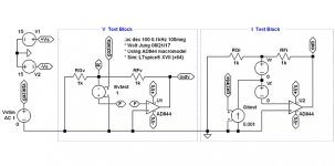
You are probably referring to the DIT test in #1704.
This is the DIT test as Middlebrook has designed, including R2.
One is Rf and the other one is Rg.
Tell me what you would like to do with R2, and I'll do it for you.
Hans
Last edited:
Try this (in a discrete CFA amplifier):You're right.
To confirm my suspicion I tried this with a LT1395 with Rg=50 Ohm and Rf=350 Ohm and by placing a cap parallel to Rf I ran into oscillations.
Because Rf is in par. with Z(s), the cap will try to extend the bandwidth of the CFA which is a no no.
Set the miller cap (best to minimize distortion between output and the VAS base) in order to get the max bandwidth with no bump at HF, then you can use a little cap (usually around 10pF) in // with the serial feedback resistance to optimise little signal square waves with no overshoot.
Done.
My two cents.
If you do that, on a CFA you mostly put a zero in the loop gain up at HF and you get oscillation.
If you have overcooked MC on a CFA, you may get away with it, but its very suboptimal then.
On a VFA, this technique works because you increase the gain margin, and this improves the transient response - as evidenced by the square wave performance. But, if you make the cap too high in value, you will run into oscillation as well.
So, on a VFA, sim and then test with a square wave stimulus to make sure you have optimized it.
On a CFA, do not do this.
Above referring in both cases to discrete designs.
That's exactly how I see it 😀If you do that, on a CFA you mostly put a zero in the loop gain up at HF and you get oscillation.
If you have overcooked MC on a CFA, you may get away with it, but its very suboptimal then.
On a VFA, this technique works because you increase the gain margin, and this improves the transient response - as evidenced by the square wave performance. But, if you make the cap too high in value, you will run into oscillation as well.
So, on a VFA, sim and then test with a square wave stimulus to make sure you have optimized it.
On a CFA, do not do this.
Above referring in both cases to discrete designs.
Post 1668 is touching a different subject.
You are probably referring to the DIT test in #1704.
This is the DIT test as Middlebrook has designed, including R2.
One is Rf and the other one is Rg.
Tell me what you would like to do with R2, and I'll do it for you.
Hans
Hans, Middlebrook does not ask that any passive components be added. All he asks is to set the input signal to zero and insert a voltage source in one case, and a current source in another. Any components added beyond these change the circuit under test.
Why don't you try at least to simulate it ?On a CFA, do not do this.
I have several CFA (laterals power fets) perfectly stable tuned this way.
Last edited:
I showed this simulation some weeks ago :Figure 2 indicates that the Amp output buffer sinks current into itself as sourced by the inverting terminal. This indicates that current reversal only occurs in the output buffer. CFA's works on the principle of shunting current away from inverting terminal current, not by feeding current into it.
An externally hosted image should be here but it was not working when we last tested it.
My approach makes clear how the unavoidable voltage difference between i+ and i- is sensed.I consider that considerable confusion exists by failing to identify the input network as a "current sensing output buffer". Although this might suggest some form of voltage feedback amplifier this isn't considered true.
I'm more than willing to try this after I already tried with the LT1395.Why don't you try at least to simulate it ?
I have several CFA (laterals power fets) perfectly stable tuned this way.
Send me a CFA of your own and I will show the results.
Hans
Chris,Hans, Middlebrook does not ask that any passive components be added. All he asks is to set the input signal to zero and insert a voltage source in one case, and a current source in another. Any components added beyond these change the circuit under test.
look at the Middlebrook layouts below.
The certainly have an Rf and a Rg.
But send me what you want to see for Rf and Rg and I'll do a sim for you.
Hans
Attachments
- Home
- Amplifiers
- Solid State
- Current Feedback Amplifiers, not only a semantic problem?