Phase and frequency are the same information, one is the derivative of the other.
Often in a PLL, the output is fed through a frequency divider or is heterodyned before being applied to a phase comparator, which is operating at a different frequency from the output. That phase is definitely not the integral of the output frequency and is not "the same information".
I could also apply the PLL output to a simple frequency to voltage converter and apply that voltage to a standard op amp error amplifier. Its output could drive a V to F converter to generate the PLL output.
I could go on. But the point is that controlling signal type A in no way requires you to feed back signal type A to the error amplifier.
The feedback path distinction being debated here is essentially about impedance; when it's high it's being called VFB and when low it's being called CFB. Where is the boundary?
I disagree. Impedance magnitude is associated with certain CFA and VFA input stages, but it is hardly the main distinguishing feature. Among the distinguishing features are bandwidth variation over a certain range of closed loop gains, and slew rate assist on demand.
I have built out of discrete components two otherwise very similar amplifiers, one a CFA, and the other a VFA. They clearly demonstrate the bandwidth variations I mentioned. Please see part 1 of https://www.audioxpress.com/article/current-feedback-fake-news-or-the-real-deal .
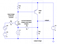
The basic configuration is a voltage divider or a direct connection to the output. Why didn't you use one the them, I don't know. Don't mind, as you see in my previous post, I finally understood that Rf it is a conceptual resistor seen by the input emitter.The additions of a DC current source and Rf make the circuit "unclear"? Rf is a part of every CFA op amp circuit! And the DC current source allows for greater variability in the selection of the value of Rf.
If this basic configuration is unclear to you, then I begin to understand why we see things so differently.
You sent your message just after mine, so you have not read it before writing yours. I think that my message will make my point of view clearer.Please refer to my schematic. AC current flows through the input collector, correct? It must also flow through the associated emitter. It cannot flow through the (DC) current source, which will not pass AC signals. It must flow somewhere. If not through Rf to the output stage, then where does it go?
My understanging of a CFA with a two resistors attenuator connected between the output and ground, the mid point being connected to the inverting input circuit which is made of one or two emitters, is :If you tell me it does not flow through the output stage, then I will bother you no more. It will have become apparent that there is too big a gap to bridge in our understandings of elementary electronics.
Current of the output flows in its load and in the feedback network which is part of the load, of coarse.
Current of the input emitter flows in the feedback resistor which is ground connected.
Current in this ground connected resistor is the sum of two currents.
The question is what defines the current in the collector of the input transistor ?
Which does control it ?
Elementary electronics to me.
Last edited:
The basic configuration is a voltage divider or a direct connection to the output. Why didn't you use one the them, I don't know. Don't mind, as you see in my previous post, I finally understood that Rf it is a conceptual resistor seen by the input emitter.
You sent your message just after mine, so you have not read it before writing yours. I think that my message will make my point of view clearer.
My understanging of a CFA with a two resistors attenuator connected between the output and ground, the mid point being connected to the inverting input circuit which is made of one or two emitters, is :
Current of the output flows in its load and in the feedback network which is part of the load, of coarse.
Current of the input emitter flows in the feedback resistor which is ground connected.
Current in this ground connected resistor is the sum of two currents.
The question is what defines the current in the collector of the input transistor ?
Which does control it ?
Elementary electronics to me.
One step at a time. Start with the unity gain CFA - certainly a practical circuit - the schematic for which I have provided. It has an Rf, but no Rg. The input stage signal current flows through the output stage, correct?
Seeking the flow of this input signal current desesperately (I added a bouquet of phases) :One step at a time. Start with the unity gain CFA - certainly a practical circuit - the schematic for which I have provided. It has an Rf, but no Rg. The input stage signal current flows through the output stage, correct?
Attachments

I don’t understand why you are focusing on the small signal AC currents. With steady state sign waves, the AC currents will be inversely proportional to the loop gain in any topology amplifier.
It’s when you feed the CFA with a fast rise/fall time signal that you can see the current on demand behavior. For a 1 mA standing current, it’s quite easy to get it to go to 8 mA and that is the essential point. VFA’s don’t do that and the peak current is never more than the LTP current in its classic form.
Secondly, how does this model explain gain bandwidth independence in CFA’s?
Sorry, this does not show that a CFA works like a VFA.
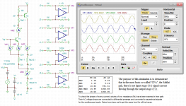
The purpose of the simulation I did has no relation with your comments.I don’t understand why you are focusing on the small signal AC currents. With steady state sign waves, the AC currents will be inversely proportional to the loop gain in any topology amplifier.
It’s when you feed the CFA with a fast rise/fall time signal that you can see the current on demand behavior. For a 1 mA standing current, it’s quite easy to get it to go to 8 mA and that is the essential point. VFA’s don’t do that and the peak current is never more than the LTP current in its classic form.
Secondly, how does this model explain gain bandwidth independence in CFA’s?
Sorry, this does not show that a CFA works like a VFA.
Seeking the flow of this input signal current desesperately (I added a bouquet of phases) :
Please don't waste your time applying my comments to your circuit. Instead, as I had requested, comment on their application to the more general case of the circuit I previously posted, and which I post again for your convenience.
It is not that your circuit is not a CFA; it is! However, it is a limited, degenerate version thereof in which Rf is constrained to equal zero. Every commercially available CFA op amp recommends the use of a non-zero Rf. Considering only Rf = 0 helps to prevent you from seeing the wider picture that would better explain the circuit's operation, whether Rf is zero or not. Your conclusions must apply to all CFA's regardless of the value of Rf, right?
Please consider the more general case of a CFA with an Rf, and (at least at first) with no Rg. Once that is addressed, you can always add an Rg, and even revisit the degenerate case of Rf = 0.
Attachments
vzaichenko,
How can you say that? There are two impedances of importance, the one represented by the low value source resistor over which the enfeebled feedback signal emerges, encountering the original signal at the low impedance-low dopant density terminal of the P-N junction diode (the other one) resulting in low intensity-low distortion interactions. Feedback signal strength and impedance ratio are irrelevant for the definition, the feedback resistor can be zero ohm.
The situation is very different at the high impedance-heavily doped-highly sensitive-high-distortion opposite pole of the diode (gate).
In the case of CFA, the feedback signal components enter at small, less damaging phase angles, as oppose to the very large, distortive phase angles occurring in the differential topology.
Go for the VFA if you believe that high gain and accurate voltage regulation give low distortion as asserted by Control Theory.
Sensitivity of the inputs is the same.
How can you say that? There are two impedances of importance, the one represented by the low value source resistor over which the enfeebled feedback signal emerges, encountering the original signal at the low impedance-low dopant density terminal of the P-N junction diode (the other one) resulting in low intensity-low distortion interactions. Feedback signal strength and impedance ratio are irrelevant for the definition, the feedback resistor can be zero ohm.
The situation is very different at the high impedance-heavily doped-highly sensitive-high-distortion opposite pole of the diode (gate).
In the case of CFA, the feedback signal components enter at small, less damaging phase angles, as oppose to the very large, distortive phase angles occurring in the differential topology.
Go for the VFA if you believe that high gain and accurate voltage regulation give low distortion as asserted by Control Theory.
Seeking the flow of this input signal current desesperately (I added a bouquet of phases) :
It seems clear that the signal current through the Rf is the same as the signal output collector current of the input stage, except for a small difference which of course is Ib (transistor appears to have hfe of 100). AM1 = AM2.
QED.
Jan
Last edited:
My comments and simulation are in contradiction with yours.Please don't waste your time applying my comments to your circuit.
Remember you request :Instead, as I had requested, comment on their application to the more general case of the circuit I previously posted, and which I post again for your convenience.
My answer is clear : I did not find anything which may show that.One step at a time. Start with the unity gain CFA - certainly a practical circuit - the schematic for which I have provided. It has an Rf, but no Rg. The input stage signal current flows through the output stage, correct?
So it obeys to today's definition of CFA, for which I invented a new name Low Impedance Inverting Input Amplifier, LIIIA.It is not that your circuit is not a CFA; it is!
Commercial op-amps were not the object of your first request, one step at a time, right ?However, it is a limited, degenerate version thereof in which Rf is constrained to equal zero. Every commercially available CFA op amp recommends the use of a non-zero Rf.
At least, I got the point with Rf = 0Considering only Rf = 0 helps to prevent you from seeing the wider picture that would better explain the circuit's operation, whether Rf is zero or not.
As I analysed until today, yes.Your conclusions must apply to all CFA's regardless of the value of Rf, right?
There is no Rg in your circuit, is it the resistor connected to the output in the feedback voltage divider for voltage gains higher than 1 ?Please consider the more general case of a CFA with an Rf, and (at least at first) with no Rg. Once that is addressed, you can always add an Rg, and even revisit the degenerate case of Rf = 0.
Why some people persistent about CFA definition, this is industry accepted nomenclature, good enough for me.
Why some people persistent about CFA definition, this is industry accepted nomenclature, good enough for me.
Because they do not understand how it work 😉
Btw, my friend finished CFA amplifier with OITPC compensation in stereo. Saturday, we will test how it sound together.
Enchanting Controversial Sonnet
Currents do not flow.
Currents do not return.
Currents do not go anywhere.
Currents do not drive currents.
Currents do not drive voltages.
Currents do not drive anything.
Currents cannot be sensed.
Currents cannot be sourced.
Currents cannot be dumped.
Currents cannot be fed back.
Eternal loving Providence shines forth resplendent
Bringing deliverance to all.
Such a miraculous spectacle.
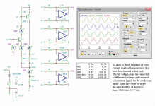
New schematics correcting the value metionned for the input signal, it was 1V RMS. I also added a short note on the purpose of the schematics.
You have proven my point. Remove R4 and you don't have an output stage - you don't even have a properly functioning circuit! Therefore, R4 is part of your output stage, which needs a return to V- of some kind to work. And the input stage current clearly flows through that output stage.
Will you please, please address your analysis of my comments to the circuit I sent you? In it, R2 is part of the output stage. Capacitively couple an additional load to ground if you feel the need. I asked you repeatedly to comment on the application of my comments to the circuit I provided. It is disingenuous to continue to apply them to a circuit they were not meant for.
Actually, your sim confirms my claim and contradicts yours. Please see my prior post.My comments and simulation are in contradiction with yours.
Your output stage will not function without your "load" resistor, of which therefore it is an inextricable part. And clearly, the input stage current flows through that "load", and therefore the output stage. And so the sim contradicts your claim.My answer is clear : I did not find anything which may show that.
Not sure what is your claim for "today's definition of CFA". I assume LIIIA is a jest.So it obeys to today's definition of CFA, for which I invented a new name Low Impedance Inverting Input Amplifier, LIIIA.
Correct. But your conclusions about CFA's must apply generally, no?Commercial op-amps were not the object of your first request, one step at a time, right ?
I am amused that you would quote "one step at a time" when so far, you have not taken that step, which involves the circuit I presented!
?At least, I got the point with Rf = 0
Please reconsider.As I analysed until today, yes.
The Rg I refer to would be connected to the input stage emitter.There is no Rg in your circuit, is it the resistor connected to the output in the feedback voltage divider for voltage gains higher than 1 ?
Enchanting Controversial Sonnet
Currents do not flow.
Currents do not return.
Currents do not go anywhere.
Currents do not drive currents.
Currents do not drive voltages.
Currents do not drive anything.
Currents cannot be sensed.
Currents cannot be sourced.
Currents cannot be dumped.
Currents cannot be fed back.
Eternal loving Providence shines forth resplendent
Bringing deliverance to all.
Such a miraculous spectacle.
What, no Haiku? 🙂
Because the industry accepted nomenclature obeys to marketing services and does not necessarily choose the adequate name for a topology.Why some people persistent about CFA definition, this is industry accepted nomenclature, good enough for me.
Currently it is the topic. Some people already gave their point of view with arguments, it would interesting you give yours, and even more interesting, how you justify it.Because they do not understand how it work
- Home
- Amplifiers
- Solid State
- Current Feedback Amplifiers, not only a semantic problem?