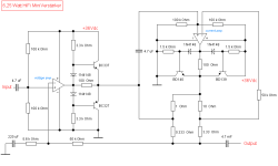
Very insightful explanation. Base on that, I come up a calibration method that you can tune the feedforward resistor until all the injected "distortion" is gone.it becomes clear that in a current dumping amplifier, any residual distortion appearing (after applying negative feedback) at the output of the current dumper Tr1 Tr2 (point D in the schematic above) is fed to the load via two parallel branches: (1) via L1; and (2) via the integrator A R1 C1, followed by R2.
If these two branches feed the load with the distortion of equal amplitude and opposite in phase, the load will see zero distortion.
If you start with the circuit in the OP, to calibrate:
1. Ground the input. Disconnect the load(speaker).
2. Inject "Error" signal as below to the output of the dumper. A serial resistor is required. Make sure the peak voltage is less than the threshold voltage of the dumper.
3. Scope the output, while adjusting R3 until all the signal is gone.
[EDIT] New version circuit fixed some issue caused by opamp non-zero output impedance.
Last edited:

Hello @jxdking
You seduced me like Eve seduced Adam ...
I've now spent a few hours in front of the stupid screen and my old SPICE - yes, current dumping (feedforward) works. But why are we playing? Probably the puzzle is tempting us ..!
In the end, I wasn't satisfied with the result either, but it was only supposed to prove that it works and it does.
I played a little further and the OP-Amp's as starting points of the exercise converged to another known concurrence concept, which can also correct even a currentless push-pull output stage almost completely.
Perhaps the last state, late at night (with no more thinking left), is also an incentive for you, with or without a dumper.
regards,
HBt.
Attachments
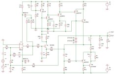
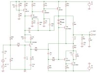
I repost the Quad 405 schematic as well as a slightly modded version, as you can see the amp and OS are strictly
the same with same VAS current, but no FFWD at all while two low drop diodes set the OS bias at 6.6mA,
only the upper device is on as on the negative side those 6.6mA are drained by the driver.
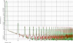
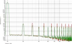
The FFT show the THD at 14V pk, in red the original amp and in green the modded and 6.6mA half biased one.
Also without L2 the amp is not perfectly stable in both cases, but anyway 5mA Iq is enough to get the same results
while using the same schematic.
As for using an opamp as driver that s the same if not worse, an EF1 biaised at 500uA bias is much better than this
half legged FFWD, and with an EF2 900uA are enough to vastly outperform the FFWD scheme also using an EF2.
Notice that those 900uA flow entirely in the drivers of the EF2, the power devices still being off.
the same with same VAS current, but no FFWD at all while two low drop diodes set the OS bias at 6.6mA,
only the upper device is on as on the negative side those 6.6mA are drained by the driver.
The FFT show the THD at 14V pk, in red the original amp and in green the modded and 6.6mA half biased one.
Also without L2 the amp is not perfectly stable in both cases, but anyway 5mA Iq is enough to get the same results
while using the same schematic.
As for using an opamp as driver that s the same if not worse, an EF1 biaised at 500uA bias is much better than this
half legged FFWD, and with an EF2 900uA are enough to vastly outperform the FFWD scheme also using an EF2.
Notice that those 900uA flow entirely in the drivers of the EF2, the power devices still being off.
Attachments
Last edited:
@wahab, adding tiny bias to quad 405 is relatively easy. As I posted before, even tiny biased class B improve THD a lot. You may keep the feed forward resistor, that would make this even better.
For the opamp version, in order to put any bias, I have to add ether bootstraps or current sources on both pos and neg rail to pull up and down the bias network. Also, extra emitter resistors are required to prevent thermal run away. Quad 405 is so thoughtful that it includes one emitter resistor R36 in original circuit even it doesn’t really need it at the first place.
I won’t bother to bias the opamp version.
I don't know if it is true, but I wouldn't be surprised if the differences were larger at lower levels, levels that just make the amplifier pass through the dead zone of the dumper. The amplifier spends a larger part of each cycle in the crossover region then.
One thing has to be said honestly about the 405:
The circuit is pretty crazy, an integrator followed by a first-order low-pass filter with a cut-off frequency of less than 50kHz, Q1 closes seamlessly as a voltage-amplifying stage in an emitter circuit whose emitter electrode acts as an input for the gnfb. Its collector load is low, i.e. a quasi current source as a working resistor - the result is a very large single-ended open-loop gain. Q3 and Q4 cause a level shift and (load-free) decoupling, i.e. a cascaded EF (a classic impedance converter, a kind of Darlington). Q5 and Q6 now form a compound darlington (100% local negative feedback, i.e. very linear). The emitter of Q6 forms the actual output node of the power output stage. This output node now feeds the equivalent PNP transistor from Q7 and Q8 - resulting in a quasi-complementary output stage in B mode.
Q1 is somehow everything at the same time, it is a phase inversion stage as well as the main node for the important control difference formation. If you simplify the jumble of lines, you are left with a very familiar structure, namely the JLH-69 (also known as the output stage in the famous TTL logic circuits ...).
What is the task of the integrated OP-Amp as the upstream stage? It adds the input current with the current required for offset correction, but it also supplies the voltage-amplifying main part formed from Q1 and consorts, completely independently of the actual amplifier ..!
1 + R28/R10 = 3.8
To be honest, this setup is an extremely negative feedback amplifier. The first part inverts, amplifies up to the rail limit (of the op-amp) and ensures continuous offset correction of the second, also inverting part.
Totally crazy, and that's what makes this legend so appealing, no more and no less. The slogan “Current Dumping” is and was nothing more than a marketing gag.
Sorry,
HBt.

thx to wahab 👍
The circuit is pretty crazy, an integrator followed by a first-order low-pass filter with a cut-off frequency of less than 50kHz, Q1 closes seamlessly as a voltage-amplifying stage in an emitter circuit whose emitter electrode acts as an input for the gnfb. Its collector load is low, i.e. a quasi current source as a working resistor - the result is a very large single-ended open-loop gain. Q3 and Q4 cause a level shift and (load-free) decoupling, i.e. a cascaded EF (a classic impedance converter, a kind of Darlington). Q5 and Q6 now form a compound darlington (100% local negative feedback, i.e. very linear). The emitter of Q6 forms the actual output node of the power output stage. This output node now feeds the equivalent PNP transistor from Q7 and Q8 - resulting in a quasi-complementary output stage in B mode.
Q1 is somehow everything at the same time, it is a phase inversion stage as well as the main node for the important control difference formation. If you simplify the jumble of lines, you are left with a very familiar structure, namely the JLH-69 (also known as the output stage in the famous TTL logic circuits ...).
What is the task of the integrated OP-Amp as the upstream stage? It adds the input current with the current required for offset correction, but it also supplies the voltage-amplifying main part formed from Q1 and consorts, completely independently of the actual amplifier ..!
1 + R28/R10 = 3.8
To be honest, this setup is an extremely negative feedback amplifier. The first part inverts, amplifies up to the rail limit (of the op-amp) and ensures continuous offset correction of the second, also inverting part.
Totally crazy, and that's what makes this legend so appealing, no more and no less. The slogan “Current Dumping” is and was nothing more than a marketing gag.
Sorry,
HBt.
thx to wahab 👍
Last edited:
That was my quick analysis, all without the dumper circuit and the very elaborate, extensive frequency response compensation - all of which adds up to the magic of Mr. Walker and his amplifiers.
Magic.
Magic.
To be honest, this setup is an extremely negative feedback amplifier. The first part inverts, amplifies up to the rail limit (of the op-amp) and ensures continuous offset correction of the second, also inverting part.
I'm pretty sure the discrete stage from base of Q1 to output is non-inverting. Note that it provides non-inverting feedback bias to the opamp's inverting input. Overall gain from C1 to speaker output is inverting.
For an analysis of the QUAD 405 DC feedback loop/second-order Butterworth subsonic filter, see https://www.diyaudio.com/community/threads/redesigning-quad-405-dc-bias-loops.339643/post-5836838 It's very easy and good for reliability to get rid of the electrolytic capacitor in the DC feedback, if you use an op-amp with negligible bias current (such as a FET op-amp).
Quad 405 is very well designed. Here is my analysis.
Based on the original circuit posted in #83, 47 Ohm feedforward resistor with 3 uH inductor, the corner frequency is about 2.5MHz. That is very aggressive considering the fT of the original output transistors is only about 5MHz.
At 20KHz, the impedance of the inductor is about 0.38 Ohm. With 100W into 8 Ohm, 5A peak, the current passing through the 47 Ohm is about 0.38/47*5 = 40ma peak. That is -40ma to +40ma before we consider any offset. During the positive swing, the offset is about 3 pn junctions (2 diodes plus 1 output transistor), so the max current on the resistor during the positive swing is 40ma + 3x0.7/0.047 = 85 ma. During the negative swing, the offset is 1 positive pn junction, so the max current on the resistor during the negative swing is -40ma + 0.7/0.047 = -25 ma.
The VAS is single ended. It can feed almost unlimited current, but it can only sink about 50ma provided by the bootstrap. The offset on the 47 resistor is very smart. It essentially offset the current requirement of the 47 Ohm feed forward resistor.
Last edited:
Dear @wahab,I don't know if it is true, but I wouldn't be surprised if the differences were larger at lower levels, levels that just make the amplifier pass through the dead zone of the dumper. The amplifier spends a larger part of each cycle in the crossover region then.
can you please do me a favor (then I don't have to type the Quad-405 into my simulator!) and compare the following points with your existing model and post them here?
Pout = 500mW, 1W, 2W, 5W, 10W at 4Ohms and 8Ohms respectively with
f0 = 100Hz, 1kHz, 5kHz, 10kHz as well as with and without feedforward R = 47 Ohm.
FFT as above too!
Many thanks in advance.
Greetings,
HBt.
🙂
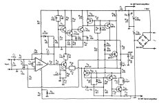
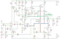
Perhaps it would help to mark the individual paths and also the standard bootstrap.
A pretty jumble ...
- red shows us the equivalent single-ended class A voltage amplifier component
- blue shows the low-impedance (because of strong negative feedback) section with transfer problems
- green, blue and red indicate the path of the dumper, the classic bridge structure (if you like to put it that way)
A pretty jumble ...
Attachments
Dear @wahab,
can you please do me a favor (then I don't have to type the Quad-405 into my simulator!) and compare the following points with your existing model and post them here?
Pout = 500mW, 1W, 2W, 5W, 10W at 4Ohms and 8Ohms respectively with
f0 = 100Hz, 1kHz, 5kHz, 10kHz as well as with and without feedforward R = 47 Ohm.
FFT as above too!
Many thanks in advance.
Greetings,
HBt.
🙂
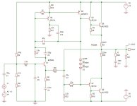
Once i have some time i ll do some comparisons between the original and the same driver using a regular QC and an EF2
as well as checking a TMC implementation, in the waiting here a paper from Wireless World with a mathematical analysis
and measurements on the first 405 version at various powers and frequencies.
Attachments
Last edited:
Then we're all looking forward to the (your) simulation results - I'm looking forward to it.
Thanks for the paper,
I had already looked for it, and I have a printout of it lying around somewhere at home (in the creative chaos).
Thanks for the paper,
I had already looked for it, and I have a printout of it lying around somewhere at home (in the creative chaos).
Some sims of the Quad inner amp, since that s the actual amp, and a simplified version using a regular QC
with no FFWD, original is the red traces, the numbers talk by themselves.
with no FFWD, original is the red traces, the numbers talk by themselves.
Attachments
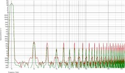
Yes, they show that your simulated QUAD 405 is well within spec. The distortion spec is < 0.01 % Dtot at 100 Hz and at 1 kHz, < 0.05 % Dtot at 10 kHz at any power level up to 100 W into 8 ohm, same distortion at the same voltage level into 8 ohm plus a reactance, and < 0.01 % on any programme signal with a rate of change smaller than 0.1 V/us at the amplifier input.
https://www.manualslib.com/manual/407305/Quad-405.html?page=5#manual
The simulations say nothing about how well or how poorly the feedforward distortion compensation works as you compare two different output stages, one in class C, the other in class AB.
The class AB circuit is not suitable for mass production, as the quiescent current depends on the matching between four different types of semiconductor devices. It can easily be solved with a VBE multiplier, but then you have the trimming point back. With or without VBE multiplier, you get the usual issues with quiescent currents that vary with programme dynamics due to imperfect thermal tracking.
To add to the confusion:
This is the common European definition!
We all know now, at least since Douglas Self, that the British idea of the optimum BIAS bias voltage leads to B operation. AB is everything between this definition of B operation and A operation.
Not a single Quad current dumper 405 is really C, but always B, optimally prebias it would already be an AB. According to Self, however, a B, for Marcel a C.
perfect world of audio,
kindly
HBt.
☕
- A Iq greater than the maximum required peak load current
- AB Iq less than the maximum required peak load current but greater than 5 to 10mAdc
- B quasi Iq = 0 mA, for battery-operated, mobile devices
- C currentless, there is absolutely no Iq, switching operation
This is the common European definition!
We all know now, at least since Douglas Self, that the British idea of the optimum BIAS bias voltage leads to B operation. AB is everything between this definition of B operation and A operation.
Not a single Quad current dumper 405 is really C, but always B, optimally prebias it would already be an AB. According to Self, however, a B, for Marcel a C.
perfect world of audio,
kindly
HBt.
☕
- Home
- Amplifiers
- Solid State
- Current Dumping with OPAMP