What is the AC current of U1 output and what is the AC current Q1 and Q2 at say half power or even to clipping.
Talking about the model in post #59
Just put current meters on the output of U1 and Q1 , Q2
bring it up to half and full power and post the AC current.
Just put current meters on the output of U1 and Q1 , Q2
bring it up to half and full power and post the AC current.
The output is about 10Vp, 20KHz. The opamp is almost running out of current with single pair of transistors, so I didn't go any higher.
The slew rate is about 2.6V/us measured. As said, if the THD is low, you should not observe high slew rate. The formula for the slew rate is: (Vin_pos - Vin_neg)*gm/Cdom. (...)
SR = 2 * PI * f3 * Vp
1.26 [V/µsec]
(valid for sinewave, spectrally pure!)
#
I love theorizing! And I maintain that a considerable bandwidth limitation (of the permissible input signal) will be necessary if the SR of the "let's say two" amplifiers should be as low as propagated.
Didn't we already have a very insightful Current-Dumper discussion thread a little while ago, with an intuitive explanation-understanding approach?
HBt.
Attachments

Aren't you implying some kind of attempted fraud?(...) So the combination is nothing else than 99.99% NFB and eventualy 0.01% error margin.
Wouldn't this have been debunked by mathematically (algebra) gifted engineers in the last few eons?
Sometimes, as we all know, people like to trick themselves. I myself am fascinated by the current-dumper principle.
What’s the signal you used to test? 20K, full power?The result is slightly lower crossover distorsion, wich is indicative that the FFWD scheme actualy worsened
The formula in #40 is based on ideal components. Thus, the impedance of L is the AC impedance only, that depends on the frequency. The finite open loop gain A is also frequency dependent. See detail in #40. The last formula in #40 is the only thing you need to calculate the optimal feedforward resistor value by given L.In the latter case, with the correct inductor DC resistance that is supposed to balance out the finite DC gain of the amplifier?
The output is about 10Vp, 20KHz. The opamp is almost running out of current with single pair of transistors, so I didn't go any higher.
The slew rate is about 2.6V/us measured. As said, if the THD is low, you should not observe high slew rate. The formula for the slew rate is: (Vin_pos - Vin_neg)*gm/Cdom. You have less error to start with, you don't need big slew rate.
View attachment 1386370
14V pk for the Quad 405, with the exact schematic.Or just large enough to activate the dumpers? Real measurement or only a simulation? In the latter case, with the correct inductor DC resistance that is supposed to balance out the finite DC gain of the amplifier?
1kHz.What’s the signal you used to test? 20K, full power?
Also for your schematic in post 59 if you remove R3, replace L1 by a short and bias the OS at a tiny 500uA
then at 1.6V pk output crossover distorsion will be 10dB lower, at 110uA bias it will still be 6dB lower.
#59, is with 6Vp input, 10Vp output. I run simulation with the same signal so that you can have thd comparison.Also for your schematic in post 59 if you remove R3, replace L1 by a short and bias the OS at a tiny 500uA
then at 1.6V pk output crossover distorsion will be 10dB lower, at 110uA bias it will still be 6dB lower.
16ma bias, without feedforward resistor. Not bad.
With the feedforward resistor. We have to admit it does something.
Aren't you implying some kind of attempted fraud?
Wouldn't this have been debunked by mathematically (algebra) gifted engineers in the last few eons?
Sometimes, as we all know, people like to trick themselves. I myself am fascinated by the current-dumper principle.
Not fraud but the difficulty to create a really analytical modelisation that accurately take account of all factors.
FI for the Quad the amp has not the OS actualy switched off, at idle the negative rail driver is active along with the VAS,
this is the same case as an EF2 biaised with +-1V, the power devices are off but not the drivers that will output say 4mA
if the power devices have 100R from their bases to the amp output, when amplitude is very low it will work as an EF1
thanks to the drivers being on and hence feedforwarding the signal through the 100R resistances up to 8mA in class A.
@jxdking, i m talking of comparing your post 59 circuit with the same circuit but with feedforward removed and the OS
biaised at 500uA and 110uA, here you also biaised the feedfoward circuit OS, only one bias please...
Last edited:
I have no idea how to do that with you said.@jxdking, i m talking of comparing your post 59 circuit with the same circuit but with feedforward removed and the OS
biaised at 500uA and 110uA, here you also biaised the feedfoward circuit OS, only one bias please...
@jxdking
R3/R4 = kA
so
A = R3/(R4k)
Replace R4 with an ideal inductor with impedance sL and you get
A(s) = R3/(skL)
which is the transfer function of an ideal integrator to time, with infinite DC gain.
Replace R4 with an inductor with series resistance, having impedance sL + R and you get
A(s) = R3/(skL + kR)
which is the transfer function of a leaky integrator to time, with finite DC gain. Its cut-off frequency has to match the frequency at which the inductive reactance equals the resistance of the inductor.
The big promise of feedforward error correction is a complete cancellation of any distortion introduced by the output stage, while feedback only reduces it by the amount of loop gain, never eliminating it fully.
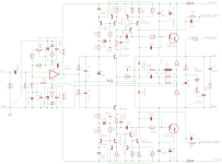
It is fairly simple to model that big promise in SPICE. Below, the two amplifiers are identical. The opamps are ideal single pole (AOL=100k, GBW=10Meg, zero output impedance), the inductors have DC resistance, everything else is visible on the schematic:. (Values can be calculated e.g. from @MarcelvdG 's formulae above). The only difference between the two amps is that the upper one includes one additional resistor, R3:

That one resistor fully eliminates any distortion introduced by the output stage from the amplifier's output:

However, making this kind of cancellation happen, or even approaching it, in real life is much harder if possible at all.
It is fairly simple to model that big promise in SPICE. Below, the two amplifiers are identical. The opamps are ideal single pole (AOL=100k, GBW=10Meg, zero output impedance), the inductors have DC resistance, everything else is visible on the schematic:. (Values can be calculated e.g. from @MarcelvdG 's formulae above). The only difference between the two amps is that the upper one includes one additional resistor, R3:
That one resistor fully eliminates any distortion introduced by the output stage from the amplifier's output:
However, making this kind of cancellation happen, or even approaching it, in real life is much harder if possible at all.
Real life it just loads down the opamp more.With the feedforward resistor. We have to admit it does something.
So distortion likely go up.
In sim land probably puts enough signal past the inductor to get lower THD
If the Fourier actually accounts for inductance and capacitance.
I probably just ignore the dc resistance of the inductor. Just matching the slope of the opamp transfer function is more practical.Replace R4 with an inductor with series resistance, having impedance sL + R and you get
A(s) = R3/(skL + kR)
which is the transfer function of a leaky integrator to time, with finite DC gain. Its cut-off frequency has to match the frequency at which the inductive reactance equals the resistance of the inductor.
That was posted in this thread :The big promise of feedforward error correction is a complete cancellation of any distortion introduced by the output stage, while feedback only reduces it by the amount of loop gain, never eliminating it fully.
Attachments

Post #67 was related to the QUAD 405. I vaguely remember having read somewhere that the QUAD 405 corrects for inductor DC resistance by restricting the DC gain of the class A amplifier, but I may be mistaken, as it must have been decades ago.
It seems quite practical to me in a discrete implementation. With the exception of superconducting inductors working at cryogenic temperatures, any practical inductor will have a DC resistance and any practical amplifier will have finite DC gain. Why not trying to make the effects on bridge balance more or less cancel?
For an implementation with an op-amp, the open-loop corner frequency of an op-amp will typically be lower than the R/(2πL) corner frequency of the inductor, but you could fix that with a big resistor from the op-amp output to the negative input. That is, with some extra feedback to reduce the DC gain.
Here is some investigation about the current that required to drive the feedforward resistor.
Assuming the feedforward resistor is 100 Ohm, the inductor is 4.7 uH.
4.7 uH is about 0.6 Ohm impedance at 20KHz. That means the 100 Ohm feedforward resistor has to provide 0.59/100 = 0.59% of the total AC current. For 8 Ohm load driven to 16Vp, you need 2A peak. 0.59% of 2A is 12ma. There is also 0.7v DC offset on the resistor. Thus total is about 19mA passing through the resistor.
If the dumper is just a single pair of transistors with beta 100. The opamp has to provide 2A/100 = 20ma for the dumper. Thus the total current required is 19ma + 20ma = 39ma.
NE5532 is internally limited to 38ma max. Thus, with 1EF dumper, it barely can drive 8 Ohm speaker to 16Vp.
One of the enhancement is to use CFP as the dumper that I posted in #16, so that you ignore the current feeding to the dumper. In this case, you can actually have the capability to drive 4 Ohm load. 16Vp with 4 Ohm, would be 4A peak, 0.59% of 4A is 24ma. Plus 7ma DC offest, 31ma in total.
Last edited:
That piece contradicts itself. It says, correctly, that with an infinite loop gain, there would be no distortion at the output of the current dumper, so the correct R3 value in that case is infinite (that is, open circuit). In the next paragraph, it states, incorrectly, that zero distortion at the output is impossible even with infinite loop gain.That was posted in this thread
Regardless of what people say, full cancellation is possible in principle, even though it is hard to get in practice. If you rearrange the schematic like this:
it becomes clear that in a current dumping amplifier, any residual distortion appearing (after applying negative feedback) at the output of the current dumper Tr1 Tr2 (point D in the schematic above) is fed to the load via two parallel branches: (1) via L1; and (2) via the integrator A R1 C1, followed by R2.
If these two branches feed the load with the distortion of equal amplitude and opposite in phase, the load will see zero distortion.
Intuitively, since L1's impedance increases with frequency at 20dB/decade, the distortion it feeds to the load falls with frequency at the same rate and lags in phase by 90°. The same distortion coming via the integrator also falls with frequency at 20dB/decade, has a 90° phase lag, and is inverted. Since the levels are proportional and phases are opposite, with the right choice of R2, the residual distortion from the current dumper can be nulled.
The circuit is particularly easy to analyze if the gain of A is assumed to be infinite. In this case, the inverting input of A (labeled F) sees zero distortion due to the feedback via C1. If the distortion is nulled perfectly, the load (labeled L) also sees zero distortion. The distortion current via L1 then is equal to that via R2, and the distortion current via R1 is equal to that via C1. A little algebra quickly shows that this happens when the DC resistance of L1 is zero, and its inductance is L1=R1×R2×C1. In the language of Walker's AES paper, "For the linearity of Tr1 and Tr2 to be immaterial then L must equal RRC".
A non-zero DC resistance of L1 limits the current through the upper branch at low frequencies. A finite DC gain of A has a similar effect on the bottom branch. You can, in principle, match the two effects and achieve full cancellation with non-ideal inductor and integrator. That's what @MarcelvdG is talking about, and what my simulation in the post above shows.
If A is a usual single-pole compensated opamp, you may get away without R1 and C1, as the opamp already behaves more or less like an integrator. That's what @jxdking is simulating.
Last edited:
- Home
- Amplifiers
- Solid State
- Current Dumping with OPAMP