......
Anyway, I don't think I did anything stupid, but I'm pretty new at the analog side of things so I could well have. One thing I did notice is that it goes into oscillation when over-driven (ie: 1.4V at the input). The unmodified schematic does this too, so maybe it's just my SPICE models or something?
Any comments appreciated.
Thanks,
Jeff.
Jeff
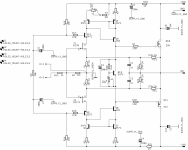
You have wrongly connected C1, R5, C3, R17 to ground instead of output. Just look carefully at circuit in first post.
I just noticed the determination of current mirrors value based on ID (thus IDSS) of the first stage which is nice🙂
Fab
Oops, I did indeed. (I wondered why adjusting the feedback didn't do what I expected.)
Thanks @fab!
Thanks @fab!
With my error fixed distortion drops a bit, I was able to adjust the feedback voltage divider to a more reasonable 270/330, and when overdriven it just clips (no oscillation).
Sweet!
Sweet!
To JeffYoung: If you want to learn about this circuit, why did you choose to argue with the designer when he pointed out some of your errors?
a) Vbe means the voltage between the base and emitter of a bjt, not "short hand" for whatever you want it to mean.
b) If you carefully read posts 1, 65, 66, 105, 106, and 265, you will see that in "shouldn't be higher than 4-5ma", juma was referring to the limits of the devices for Q5, Q8, and it is optimum to have 4-5ma per output pair, if you have multiple output pairs and want to maintain bandwidth. If you really want to understand why, Nelson's article on F5T, I think, discusses the challenges of charging the gate capacitance of multiple pairs of large mosfets. It does not help to attack juma's English.
c) Why are you arguing with juma over the minute definitions of oscillation and unstable? If an amp oscillates, then it cannot be considered very stable, now can it? These questions do not expect, nor want, a response.
d) See b.
e) This is the place to come if you do not take out of context what the designer says and then argue with the designer. If you do not want to use the circuit as is, maybe choose a different circuit where the designer has already written out how to modify it.
I mainly wrote this post for juma.
To juma: please do not let the actions of a few people stop the majority of us from learning from and enjoying your designs, knowledge and experiments. Besides, I think you will enjoy them more if you can share them with people who do want to learn. Thank you.
...
b) If you carefully read posts 1, 65, 66, 105, 106, and 265, you will see that in "shouldn't be higher than 4-5ma", juma was referring to the limits of the devices for Q5, Q8, and it is optimum to have 4-5ma per output pair, if you have multiple output pairs and want to maintain bandwidth.
Oh, excellent. I internalised the part about using a "stronger pair" at the output of the current mirror (I'm using KSA1381/KSC3503), but the part about increasing the current through them didn't to get to long-term storage.
Thanks,
Jeff.
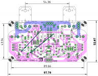
Here are the gerbers for the version with double sided pcb design, as requested by a member.Hi Gabor,
The layout you attached is correct except for K170 orientation , it should be rotated by 180deg .
here is the correct layout. if you want i could post pdf and its sch. its not tested.
A member has ordered/ going to produce double sided PCB's with re-inforced high current traces. You could contact him to get a pair for your friend. lot less hassle and a breeze to build with PCB.
regards
prasi
Attachments


Thank you Prasi!Here are the gerbers for the version with double sided pcb design, as requested by a member.
regards
prasi
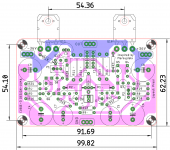
I have a question What is the voltage rating of the 100uF and 220uF (marked) capacitors? I have a lot of Silmic at hand but I can not install those because of their size. I ordered way back a lot of those Silmics they are just too big. At first I thought to make a home brew PCB so I can use use those caps I already have. The same time the home brew quality far behind your PCB. Maybe I can get some lower voltage good quality caps but smaller size. I have all the other components for the amp to test and finish her. Greetings
Attachments
Last edited:
Hello Gabor,
I think they see full rail voltage , so need be 50V atleast. and the dia of caps is 10mm.
So I think you will have limited option .
Checking mouser, we seem to have 157 options, out of which audio grade are 8 numbers.
https://www.mouser.in/c/passive-com...20 uF&diameter=10 mm&voltage rating dc=50 VDC
regards
prasi
Hello Gabor,
I can do one thing, I can extend the sides a bit to accommodate your bigger caps. Tell me the size, are they 18mm dia?
And I can quickly post the DIY pdf version so that you can use the slimics that you already have.
Let me know if any other modification in size is required.. I can do it .
regards
prasi
Hello Gabor,
I think they see full rail voltage , so need be 50V atleast. and the dia of caps is 10mm.
So I think you will have limited option .
Checking mouser, we seem to have 157 options, out of which audio grade are 8 numbers.
https://www.mouser.in/c/passive-com...20 uF&diameter=10 mm&voltage rating dc=50 VDC
re
Prasi the 100uF Silmic has 13mm and the 220uF has 16mm footprint. I do not think that 100uF next to the 220 it has to be 50V, please take a look before the cap it has an 18K resister. Maybe 25V or even less, it would be great if someone could measure it.Hello Gabor,
I can do one thing, I can extend the sides a bit to accommodate your bigger caps. Tell me the size, are they 18mm dia?
And I can quickly post the DIY pdf version so that you can use the slimics that you already have.
Let me know if any other modification in size is required.. I can do it .
regards
prasi
REMEMBER I already own a pair of your PC board, the black one but for future orders of course.

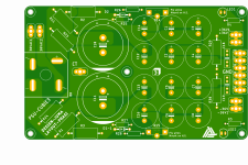
here are files including gerbers and diy pdfs
Attachments
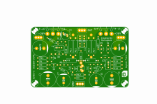
-
 cubie3-lay-ver1.2.png47.3 KB · Views: 354
 -
 cubie3-sch-ver1.2.png534.9 KB · Views: 333
 -
cubie3-ver1.2-btm-cu.pdf16.9 KB · Views: 184
-
cubie3-ver1.2-top-silk.pdf31 KB · Views: 186
-
cubie-cambe-correctedR1.2-slimic_2022-02-09.zip298.9 KB · Views: 209
-
 cubie-cambe-correctedR1.2-slimic-BTM.png314.3 KB · Views: 306
 -
 cubie-cambe-correctedR1.2-slimic-TOP.png344 KB · Views: 283

Hi prasi, thanks for the info on the amp pcb's for the Cubie 3. Back in 2018 at post #274 you show pdf's of the PSU board you did to suit this amp. Did you ever post the gerber's for this PSU pcb, if so where? If not can you post them here if you still have them thanks.
Regards,
Gary..
Regards,
Gary..
Hi Gary,
here is an improved version with GBPC3510 rectifier, on which you can place a heatsink also.
https://www.mouser.in/datasheet/2/596/SDS_ATS-X50300P-C1-R0-1385600.pdf
here is an improved version with GBPC3510 rectifier, on which you can place a heatsink also.
https://www.mouser.in/datasheet/2/596/SDS_ATS-X50300P-C1-R0-1385600.pdf
Attachments

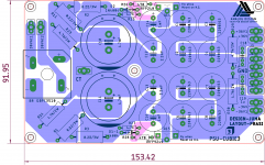
here are files for the PSU for Cubie-3.
Attachments
-
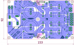 CUBIE-NEW-PSU-LAY.png66.2 KB · Views: 316
 -
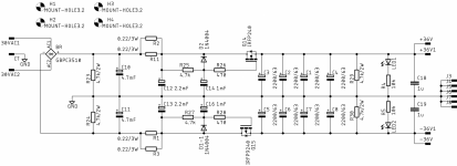 CUBIE-NEW-PSU-SCH.png237.1 KB · Views: 287
 -
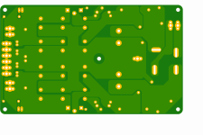 cubie-PSU.png358 KB · Views: 281
 -
cubie-PSU_2022-02-09-GERBERS.zip350.8 KB · Views: 171
-
 cubie-PSU-TOP.png516.6 KB · Views: 253
 -
cubie3 psu btm cu.pdf70.7 KB · Views: 180
-
cubie3 psu top silk.pdf42.3 KB · Views: 179
- Home
- Amplifiers
- Pass Labs
- Cubie3