Prasi- 4 nos.
Silasmellor - 4 nos.
Vunce- 4 nos.
Myint67- 4 nos
Vasilis-6
Hicoco - 2
Surfatwork - 2
manniraj - 2
Silasmellor - 4 nos.
Vunce- 4 nos.
Myint67- 4 nos
Vasilis-6
Hicoco - 2
Surfatwork - 2
manniraj - 2
Prasi- 4 nos.
Silasmellor - 4 nos.
Vunce- 4 nos.
Myint67- 4 nos
Vasilis-6
Hicoco - 2
Surfatwork - 2
manniraj - 2
Cl00sed(Rajesh) - 2
Silasmellor - 4 nos.
Vunce- 4 nos.
Myint67- 4 nos
Vasilis-6
Hicoco - 2
Surfatwork - 2
manniraj - 2
Cl00sed(Rajesh) - 2
Would you be able to supply a schematic for the new board?
I have two of you older boards and I like this even better.
I have two of you older boards and I like this even better.
Prasi- 4 nos.
Silasmellor - 4 nos.
Vunce- 4 nos.
Myint67- 4 nos
Vasilis - 6
Hicoco - 2
Surfatwork - 2
manniraj - 2
Cl00sed(Rajesh) - 2
MD_Stryker - 4
Silasmellor - 4 nos.
Vunce- 4 nos.
Myint67- 4 nos
Vasilis - 6
Hicoco - 2
Surfatwork - 2
manniraj - 2
Cl00sed(Rajesh) - 2
MD_Stryker - 4
Last edited:
Would you be able to supply a schematic for the new board?
I have two of you older boards and I like this even better.
Hello Stryker,
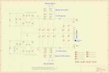
Yes, ofcourse I will post the schematic, but it needs a bit of clean up.
Probably by weekend , I will post it here.
regards
Prasi
Hello Stryker,
Yes, ofcourse I will post the schematic, but it needs a bit of clean up.
Probably by weekend , I will post it here.
regards
Prasi
Awesome. Thanks!
Prasi- 4 nos.
Silasmellor - 4 nos.
Vunce- 4 nos.
Myint67- 4 nos
Vasilis - 6
Hicoco - 2
Surfatwork - 2
manniraj - 2
Cl00sed(Rajesh) - 2
MD_Stryker - 4
xrk971 - 2
GB Update:
Prasi- 4 nos.
Silasmellor - 4 nos.
Vunce- 4 nos.
Myint67- 4 nos
Vasilis - 6
Hicoco - 2
Surfatwork - 2
manniraj - 2
Cl00sed(Rajesh) - 2
MD_Stryker - 4
xrk971 - 2
gary s - 4
Prasi- 4 nos.
Silasmellor - 4 nos.
Vunce- 4 nos.
Myint67- 4 nos
Vasilis - 6
Hicoco - 2
Surfatwork - 2
manniraj - 2
Cl00sed(Rajesh) - 2
MD_Stryker - 4
xrk971 - 2
gary s - 4
Prasi- 4 nos.
Silasmellor - 4 nos.
Vunce- 4 nos.
Myint67- 4 nos
Vasilis - 6
Hicoco - 2
Surfatwork - 2
manniraj - 2
Cl00sed(Rajesh) - 2
MD_Stryker - 4
xrk971 - 2
gary s - 4
Project16 - 2
Silasmellor - 4 nos.
Vunce- 4 nos.
Myint67- 4 nos
Vasilis - 6
Hicoco - 2
Surfatwork - 2
manniraj - 2
Cl00sed(Rajesh) - 2
MD_Stryker - 4
xrk971 - 2
gary s - 4
Project16 - 2
Hi prasi,
Good work on all of this, with the schematic when you get a chance to update and post it, can you also add a BOM for completeness if possible.
Keep up the good work..
Good work on all of this, with the schematic when you get a chance to update and post it, can you also add a BOM for completeness if possible.
Keep up the good work..
Prasi- 4 nos.
Silasmellor - 4 nos.
Vunce- 4 nos.
Myint67- 2
Vasilis - 6
Hicoco - 2
Surfatwork - 2
manniraj - 2
Cl00sed(Rajesh) - 2
MD_Stryker - 4
xrk971 - 2
gary s - 4
Project16 - 2
sorry for cut 2
Hi PrasiAlmost ready🙂.
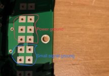
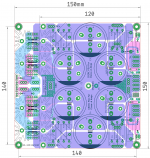
Indeed a good pcb layout. I would suggest a small change on the output ground to have a slightly higher trace return impedance for small signal ground compared to high power ground. This way it avoids more “pollution” of small signal ground by high power ground ac signal. See this example.
Fab
Attachments
Last edited:
Bonjour Prasi,
One more request if enough room, ad 1 more PCB terminal to V+ and V- and 2 more for Ground ( one Ground signal and one Ground Power )
I have to connect my Preamp and RIAA regulated Power supply
Thanks
FR

One more request if enough room, ad 1 more PCB terminal to V+ and V- and 2 more for Ground ( one Ground signal and one Ground Power )
I have to connect my Preamp and RIAA regulated Power supply
Thanks
FR
Hello Prasi
Very beautiful design with impeccable optimization of the place, I really think that this layout and improvements will make this power supply a must.
There are fuse doors the led inside that illuminates the transparent fuse can be the most beautiful effect.
Bravo! 😉
Very beautiful design with impeccable optimization of the place, I really think that this layout and improvements will make this power supply a must.
There are fuse doors the led inside that illuminates the transparent fuse can be the most beautiful effect.
Bravo! 😉
Attachments
Hello Fab, Hicoco and P16,
thank you for your comments. I have incorporated most suggestions.
P16, thanks for suggestion of fuse with led. However some may decide not to use fuse, however will want led display. For those not using fuse, J1/J2 can be populated with 1.5mm dia wire.
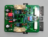
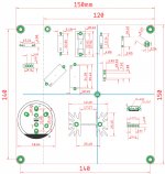
I am attaching the schematic and layout along with component dimensions.
I think this will give general idea of components to be used.
regards
Prasi
thank you for your comments. I have incorporated most suggestions.
P16, thanks for suggestion of fuse with led. However some may decide not to use fuse, however will want led display. For those not using fuse, J1/J2 can be populated with 1.5mm dia wire.
I am attaching the schematic and layout along with component dimensions.
I think this will give general idea of components to be used.
regards
Prasi
Attachments
Last edited:
Hi Prasi
Indeed a good pcb layout. I would suggest a small change on the output ground to have a slightly higher trace return impedance for small signal ground compared to high power ground. This way it avoids more “pollution” of small signal ground by high power ground ac signal. See this example.
Fab
If you want to isolate the small signal GND from dirty power GND, perhaps a 10R resistor GLB and two anti-parallel 1N4004 diodes and 22nF film cap in parallel to form the connection rather than just a thinner trace - which is so short I am not sure it will it will provide any benefit.
Hello x, hope you are doing well. And thanks for your interest .
Regarding Fabs suggestion, it's inline with what bonsai posted in the practical grounding bible.
Regards
Prasi
P.S.. see how it's away from main current traces.
Regarding Fabs suggestion, it's inline with what bonsai posted in the practical grounding bible.
Regards
Prasi
P.S.. see how it's away from main current traces.
Last edited:
Isn't the Resistor-2xdiode-cap usually used as a GLB between PSU/signal gnd and chassis (safety earth)? At least that is what appears to be the case from DIY firstwatt supplies and Rod Elliott's pages...
- Home
- Group Buys
- CRC Power Supply (Class A amplifier)