Well Russell, at that point is not a voltage gain stage anymore so calling it a VAS would be a misnomer. Driving the emitter or the source makes the second stage a current conveyor. Hence you get the high GBW.
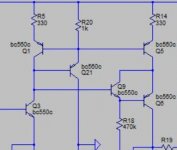
I don't think that there some circuit never seen, look this, similar Wilson with super pair (Boxal).😀
No NFB line amp (GainWire mk2)
Your circuit is not willson and not darlington. Q21 is emitter follower to provide the base currents of Q1,Q5 for perfect mirror. The voltage at collector of Q1 remains near constant to provide the cascode base Q6 a near fix low impedance voltage by Q9. In symmetric it looks very elegant circuit but far to be anything similar to mine. I wonder if it is not better to link the collector of Q9 to rail.
Attachments
Last edited:
I love cascode VAS stages, but I gave up driving the base of the VAS stage a long time ago (20 years). Now I drive the emitter (or source, if it's MOS) of the cascode transistor directly from the diff-amp output. I get a much higher GBW product.
Nad has such amp where the VAS stage has disappeared, leaving the amp 2 stages, more such amps are Unusual amp from 1987
Why unusual ? Conventional amplifiers with very deep common OOS with a linear cascode voltage amplifier .Nad has such amp where the VAS stage has disappeared, leaving the amp 2 stages, more such amps are Unusual amp from 1987
And what is VAS ?I'm a little confused about your terminology.
The title of the thread is "Unusual amp from 1987". Ask Minek about it.
The three stages are abbreviated as IPS, VAS, OS used in amplifier related literature, as input stage, voltage amplifier stage, output stage.
The three stages are abbreviated as IPS, VAS, OS used in amplifier related literature, as input stage, voltage amplifier stage, output stage.
Nad has such amp where the VAS stage has disappeared, leaving the amp 2 stages, more such amps are Unusual amp from 1987
In the above schematic, Q313/Q315 fulfill the role of VAS.
Why do you say it 'disappeared'?
True. That's the title 🙂The title of the thread is "Unusual amp from 1987". Ask Minek about it.
But it wasn't "unusual" because it didn't have VAS..
All the amps in that thread have VAS, just slightly different than typical, Miller compensated VAS in blameless topology.
There is certain similarity between the NAD amp shown above, and these amps from 'unusual' thread.
In ordinary voltage amplifier it gets input voltage and amplifies to output voltage of very high gain and it's pole. When the transistor is used in common base mode, it doesn't act as amplifier but I/V converter with extremely high pole equal to its Ft, in cascode . By this in the transfer function it disappears, and the 3 stage amplifier behaves as 2stage. If CFA is used which makes the IPS disappear you will be left with OS transfer function alone as single stage.
Last edited:
In the above schematic, Q313/Q315 fulfill the role of VAS.
Why do you say it 'disappeared'?
Hi Minek, Q313 / Q315 are folded cascode transistors. Essentially current conveyors and provide no voltage amplification. Therefore, they are an extension of the input stage.
The best way to see it, is to count high impedance nodes. In this amplifier there is only one.
Is this a VAS ?
Attachments

Last edited:
Hi Stanislav,
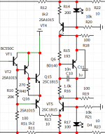
1. Circuit 1: What is before VT1?
2. What is input and what is output?
Hard to tell without seeing the whole circuit.
1. Circuit 1: What is before VT1?
2. What is input and what is output?
Hard to tell without seeing the whole circuit.
Generally speaking devising amp to a IPS, VAS and OS is just for the purpose of better understanding of specific function of a stage. IPS provides high impedance low noise interface for the input signal and return from global feedback. VAS has to provide full peak to peak voltage swing. OS provides enough current for driving the load.
In real world projects, stage names are not always in accordance with the strict definition. More over, there are many designs where these functions are combined. Extreme case is Zen amplifier where single active device serves all three purposes.
In real world projects, stage names are not always in accordance with the strict definition. More over, there are many designs where these functions are combined. Extreme case is Zen amplifier where single active device serves all three purposes.
Is this a VAS ?
Hi Stanislav,
Circuit 1 is a folded cascode VAS preceded by an over-complicated multi-stage level-shifting buffer. It doesn't seem like VT2, Q15, and Q16 will turn on, so this one is probably dead in the water.
Circuit 2 is not a VAS, but a current-boosted buffer stage. At least it wants to be.
R6 and R7 should be tied to the rails.
R8 - R10 are actually clever, separating the setting of the quiescent bias from the large signal current.
There's no reason for Q4, Q5, and Q7 - Q12 to exist. Their only function is to double the current of Q3 and Q6. A function better handled by doubling R11 and R15.
I agree with chip that there's no reason for R12 - R14 to exist. Just short them all.
Current conveyor?
Actually, it is called a folded cascode when you do that.
Well Russell, at that point is not a voltage gain stage anymore so calling it a VAS would be a misnomer. Driving the emitter or the source makes the second stage a current conveyor. Hence you get the high GBW.
Actually, it is called a folded cascode when you do that.
Disappointed. The first circuit is a voltage amplifier of a super-linear power amplifier from the reference in post 83. The second figure is a slightly simplified input stage from opamp AD 844 the input circuit and the OOS circuit are not drawn.
Last edited:
Hi Minek, Q313 / Q315 are folded cascode transistors. Essentially current conveyors and provide no voltage amplification. Therefore, they are an extension of the input stage.
Are you sure? If you check AC voltage (vs ground) on their BASES, EMITTERS and COLLECTORS - there is definitely voltage amplification.
I'm not arguing HOW voltage is amplified, but it has to be amplified SOMEWHERE, and as far as I can trust the sim, and the oscilloscope,
there is amplified voltage present on their collectors.
I treat it as VAS, with input (low voltage) at the emitter, and output at the collector. If this is a cascode or not, or if it has a pole or not, should be irrelevant.
This is just "implementation detail".
If you want to see the topology with VAS really missing - check out Ian Hegglun's 'square law amp', where voltage amplification is done in OS:
Square Law Amp
Last edited:
- Home
- Amplifiers
- Solid State
- Comparative VAS+cascode stage