Not easy to go bellow 1%, but to note that the majority of the distortion is even order. In push pull , it can be reduced to at least 50%. The complimentary pairs don't have identical collector impedance distortion.
Attachments
Last edited:
Not easy to go bellow 1%, but to note that the majority of the distortion is even order. In push pull , it can be reduced to at least 50%. The complimentary pairs don't have identical collector impedance distortion.
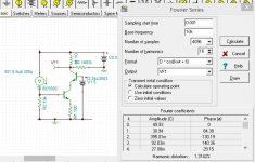
This is the LKA's output stage measured by 1M source 30+15ua 10khz for 30V out. With 2% distortion , if the VAS has 1% , It was perfectly acceptable.
Attachments
Last edited:
I passed the beta from 845 to 8450 the distortion fell from 0.06% to 0.04%.
Oh well, thought that the T4 would be limitation... I guess not.
[/Quote] The circuit on 27 is only two transistors with lower distortion but lower second pole. [/Quote]
But that circuit is not current mirror based anymore. Which is fine for the purpose of the whole thread, just not a fair comparison between the two circuits.
Anyway, how is the test done? From your settings, I make out the following, but not 100% sure:
- F=10KHz
- Vout=40V_RMS
- Driven with a current source
Anything else?
I am trying out different types of VAS+cascode stage for lowest distortion. These are the ones I tested. Please ,suggest other ones I try out.
The stage must provide a current gain of 10, to bring the 1M ohm load to +/-30v 10khz.
That is , 3u amp ac 10khz input, 30v peak output.
To make this test a bit more realistic, you need to model the second stage's (VAS) load. Else, you will be getting unrealistic numbers. I.e. you need to consider/model how well the second stage play's with the output stage... and in case you are thinking it, being cascoded is not enough to ignore the second stage load.
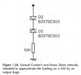
Groner suggested a circuit in one of his papers and Self has incorporated in his book in chapter 7. See attached picture.
Groner suggested a circuit in one of his papers and Self has incorporated in his book in chapter 7. See attached picture.
Attachments
A standard triple emitter followers have a current gain of 100³ . 8 ohms load than reflects to the VAS 8×100³=8 Mohm. but for current biasing issues It gets lower. LKA's OS measures 2M ohm. The load circuit presented is only 10k.
That is at DC and when the transistors have only bias current running through them. Beta drops with frequency and with collector current.
1. What is the input impedance of LKA's triple at 10KHz?
2. Also, consider doing a simple time domain test. Drive the triple with a voltage source sine wave, 30Vpp at 10KHz. See what is the current being drawn, and how distorted it is.
BTW, you never said that we should assume the second stage is driving LKA's triplet or something similar. That changes the design constraints a bit.
Last edited:
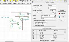
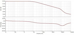
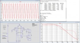
The LKA required 17ua 10khz to swing +/-30v as stand alone. Adding 1M ohms source it required 30ua for 1M ohm +15ua to swing. To note that LKA has designed for 4 ohms load, than it will become 1M ohm. See the impedance bode plot for 8 ohm load. 0db =1 ohm.
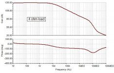
Here is the 4 ohm load. strange it doesn't goes 6db down.
The initial design consideration has always been 1M ohm load.
Here is the 4 ohm load. strange it doesn't goes 6db down.
The initial design consideration has always been 1M ohm load.
Attachments
Last edited:
Hi Hayk, I have been giving this a lot of thought. Given the topology of choice for the output stage (a triple), I think the circuit in #42 is as good as it gets for a cascoded 2nd stage (ignoring compensation which has to do more with the rest of the amp).
If you were using a double OPS (rather than triple) it would be a totally different story since loading of the 2nd stage would give you a lot more distortion that a cascode cannot correct.
If you were using a double OPS (rather than triple) it would be a totally different story since loading of the 2nd stage would give you a lot more distortion that a cascode cannot correct.
I was just curious how the VAS in my amp was doing, so I gave it a run.
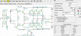
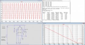
In the image below, taken at 10kHz with an input current of 40uA, with a 50pF feedback cap and loaded with a 1Meg output resistor, you see a distortion of 0.004% of which H2 is by far the biggest.
H3 is at 0.0017%.
The block below in the circuit diagram is a Wilson current mirror.
The second image shows the FR.
I see no direct reason to further tune this circuit.
Hans
Attachments
The required VAS is intended for wide band 20khz min. two pole . The VAS then functions without integrating feedback. This is why you must measure the distortion in open loop. What is A84 transistor? With the Wilson current mirror, how many transistors the circuit is made of ? The 10kHenry inductance ? The second pole is merely 3Mhz .
Last edited:
The A64 are MPSA64 Darlington's, not a very fast ones.
That's why I replaced them by 2N4403 transistors.
I also made the necessary DC Bias a lot better with the opamp.
Wilson is nothing special with 4 transistors.
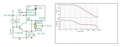
FR response is made flat up to 20kHz by inserting R4, the second pole is beyond 20Mhz.
Distortion is an unbelievable low 0.5ppm when using 50pF//100k for resp. C2 and R4.
Distortion is 1.2ppm for 20pF//600k and finally 2.8ppm for 10pF//1Meg.
Only for the last version I have inserted the images with results from the sim.
To get the +/-10V output in this image, a +/- 12uA input signal was needed.
Hans
That's why I replaced them by 2N4403 transistors.
I also made the necessary DC Bias a lot better with the opamp.
Wilson is nothing special with 4 transistors.
FR response is made flat up to 20kHz by inserting R4, the second pole is beyond 20Mhz.
Distortion is an unbelievable low 0.5ppm when using 50pF//100k for resp. C2 and R4.
Distortion is 1.2ppm for 20pF//600k and finally 2.8ppm for 10pF//1Meg.
Only for the last version I have inserted the images with results from the sim.
To get the +/-10V output in this image, a +/- 12uA input signal was needed.
Hans
Attachments
Much better. The output I measured 10khz +/-30v. As the current gain should be min 10, it must be driven by 3ua for 30ua on the load 1M. For now your current gain is less than 1.
Last edited:
Much better. The output I measured 10khz +/-30v. As the current gain should be min 10, it must be driven by 3ua for 30ua on the load 1M. For now your current gain is less than 1.
+/- 30 volt output with only a single 40 V supply in your model, how can you do that?
Getting more gain is simply a matter of lowering the value of C2, I will try how far I can go.
You never told why you need this very high gain, that would help.
Hans
In my model I replaced the CCS with an Inductor. No offset problems. The gain is modest compared to what is generally done. If the input stage has 5mS , the total becomes 50mS. With 1M ohm load gives an open loop gain of 50000. For closed looped gain of 25, it yields a NFB possible of 2000 , 66db.
Last edited:
O.k. I reduced C2 even further to 0.5pF.
I think all conditions are met, FR flat to 20kHz, second pole above 10Mhz and a current gain of 10, all with the same circuit as before.
You mentioned a distortion of 0.0012% at 27 Volt at 1kHz.
This version produces 0.0005% at that output frequency and output level.
Then you specified 0.0005% at 16 Volt at 10kHz, but I suppose that this is a typo and must be 0,005% because THD is usually higher at higher frequencies.
However, my version produces 0,002% at that output level and frequency.
When going to +/-30Volt at 10kHz, distortion becomes 0,0085%.
At 1kHz and +/- 30Volt this is 0.001%.
What still puzzles me, is that exactly C2 has usually the function of creating the dominant pole, so how realistic is this low capacitance ?
Hans
Attachments

- Home
- Amplifiers
- Solid State
- Comparative VAS+cascode stage